


Views: 0 Author: Site Editor Publish Time: 2026-05-01 Origin: Site


Modern electronics continually push the boundaries of spatial density and power output. Engineers face a constant battle against thermal degradation. We briefly define ceramic pcb fabrication as the process of building electrical circuits on inorganic dielectric substrates, like Alumina or Aluminum Nitride, instead of standard epoxy-glass like FR4.
As electronics miniaturize through Very Large-Scale Integration (VLSI) and power densities increase in IGBTs and high-power LEDs, traditional FR4 hits a functional thermal wall. FR4 traps heat and eventually fails catastrophically due to severe Coefficient of Thermal Expansion (CTE) mismatch. Component solder joints simply shear apart under continuous thermal cycling.
You need substrates capable of surviving extreme operational parameters. This guide explores the exact manufacturing processes, material choices, design constraints, and assembly realities required to successfully evaluate and procure these specialized boards. You will learn how to navigate vendor capabilities and avoid costly design errors.
Ceramic PCBs offer 20x to 100x the thermal conductivity of standard FR4, eliminating the need for bulky heatsinks in many high-power applications.
Fabrication technologies (DPC, DBC, AMB, HTCC, LTCC) dictate thermal performance, layer counts, and unit costs.
Transparent limitations: Ceramic boards are brittle, dimensionally limited, and typically constrained to 1-2 layers for optimal manufacturing yields.
PCBA on ceramic requires specialized reflow profiling due to the material’s extreme thermal mass, which can otherwise cause thermal shock to components.
Engineers default to FR4 for most basic circuit designs. It offers excellent electrical insulation and low manufacturing costs. However, FR4 becomes a severe liability in high-power applications. You must transition to inorganic substrates when thermal thresholds exceed traditional epoxy-glass limits.
High-power electronics generate immense thermal loads. Consider modern high-power LEDs. They convert up to 70% of their consumed electrical energy directly into heat. Traditional FR4 acts as a thermal insulator. Even metal-core printed circuit boards (MCPCBs) rely on dielectric epoxy layers. These epoxy layers restrict heat flow to the metal backing. Ceramic substrates remove this barrier entirely. They provide direct, unimpeded thermal pathways away from critical component junctions.
Heat dissipation is only half the battle. Temperature fluctuations cause materials to expand and contract. Silicon components expand at a specific rate. FR4 expands at a drastically higher rate. This difference is known as a CTE mismatch.
Leadless Chip Carriers (LCCs) and Surface Mount Technology (SMT) components suffer greatly on FR4 during active thermal cycling. The board expands faster than the silicon die. This tears the solder joints apart, causing premature failure. Ceramic substrates closely match the CTE of silicon. They ensure complete mechanical stability under extreme thermal stress.
Procurement teams often hesitate at the higher initial price of ceramic substrates. You must justify this fabrication cost by demonstrating broader system-level savings. Ceramic boards often eliminate the need for thermal interface materials (TIMs). They remove bulky external heatsinks. They also drastically reduce warranty failures in demanding aerospace or automotive applications. The system reliability improvements easily offset the initial board cost.
You cannot treat ceramic substrates as a monolith. Engineers choose from several distinct material formulations and metallization technologies. Each combination solves specific thermal and electrical challenges.
The base inorganic material dictates the ultimate thermal ceiling of your board. You must balance thermal conductivity requirements against material costs.
Alumina (Al₂O₃): This serves as the industry standard. It delivers a thermal conductivity of 20-35 W/mK. It works best for general high-power applications and budget-conscious thermal control.
Aluminum Nitride (AlN): This provides premium thermal management. It boasts an impressive 170-230 W/mK thermal conductivity. It offers a near-perfect CTE match for silicon. Engineers spec AlN for radar systems, microwaves, and extreme heat scenarios.
Skeptical Note: You might encounter historical references to Beryllium Oxide (BeO). It offers exceptional thermal conductivity. However, BeO dust is highly toxic. Responsible manufacturers actively phase it out. Avoid specifying BeO for new designs.
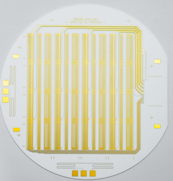
Bonding copper to an inorganic ceramic requires specialized processes. Standard adhesive pressing does not work here.
Direct Plated Copper (DPC): Manufacturers use physical vapor deposition to bond thin copper layers. DPC is ideal for high-power LEDs. It delivers excellent results for precise, fine-line trace resolutions.
Direct Bonded Copper (DBC): This uses a high-temperature oxidation bonding process between 1065-1085°C. The copper melts slightly and fuses directly to the ceramic. It proves optimal for heavy copper applications and industrial inverters.
Active Metal Brazing (AMB): This process relies on a 700-900°C vacuum brazing technique. It offers superior joint reliability. Engineers rely on AMB for rugged automotive and heavy-duty IGBT modules.
HTCC vs. LTCC: High-Temperature Co-fired Ceramic (HTCC) requires baking environments exceeding 1600°C. Low-Temperature Co-fired Ceramic (LTCC) operates at 850-900°C. LTCC minimizes tolerance shrinkage and allows the use of highly conductive metal pastes like gold or silver.
Material and Process Comparison Table
Material/Process | Thermal Conductivity | Best Use Case | Cost Profile |
|---|---|---|---|
Alumina (Al₂O₃) + DPC | 20-35 W/mK | LEDs, fine-pitch tracing | Moderate |
AlN + AMB | 170-230 W/mK | Automotive, rugged IGBTs | High |
Alumina (Al₂O₃) + DBC | 20-35 W/mK | Heavy copper power inverters | Moderate to High |
Understanding the actual manufacturing sequence builds crucial vendor trust. It demystifies why lead times differ from standard FR4 orders. Reliable Ceramic PCB Fabrication demands highly specialized, multi-stage environmental controls.
Phase 1: Substrate Preparation and Laser Drilling. Operators prepare the bare ceramic plates. They size the boards using specialized tools. Laser drilling creates precise vias. Mechanical drilling easily shatters brittle ceramics. Lasers vaporize the material safely.
Phase 2: Metallization. Manufacturers employ technologies like Laser Rapid Activation Metallization (LAM) or vacuum sputtering. These techniques bond copper directly to the inorganic ceramic. They eliminate thermal-blocking adhesive layers completely.
Phase 3: Imaging, Etching, and Plating. Facilities transfer the CAD circuit design onto the substrate. Thick-film copper processing requires specialized pure-nitrogen baking environments. Nitrogen prevents severe copper oxidation during high-temperature curing.
Phase 4: Solder Masking and Surface Finishing. Standard solder masks bubble and fail under extreme heat. Vendors apply specialized protective layers. They add surface finishes like ENIG or immersion silver. These finishes withstand high-temperature end-use environments flawlessly.
Phase 5: V-Cut and Profiling. Singulating a finished ceramic panel requires extreme care. Mechanical routing induces invisible micro-fractures. Manufacturers use precise laser V-cutting to separate the individual units safely.
Engineers often attempt to apply standard FR4 design rules to ceramic layouts. This guarantees manufacturing failure. You must design around the rigid physical constraints of inorganic substrates.
You cannot manufacture ceramic panels in standard 18x24-inch FR4 sizes. Large ceramic sheets warp violently during the high-temperature baking processes. They also shatter easily during handling. Most vendors cap maximum panel dimensions around 138x190mm. You must plan your array sizes accordingly to avoid massive yield losses.
We highly recommend restricting designs to single-sided or double-sided layouts. Multilayer ceramic PCBs certainly exist. However, the multi-stage lamination process heavily increases board shattering risks. Pressing brittle layers together drastically lowers manufacturing yields and drives up per-unit costs.
Ceramics behave like glass. They handle immense electrical pressure. An Alumina board easily withstands high dielectric breakdown voltages up to 20KV/mm. However, the material remains highly sensitive to mechanical bending. Installation technicians must avoid overtightening mounting screws. Minor impact stress or chassis torsion will snap the board instantly.
Best Practices for Ceramic Design
Keep mounting holes at least 5mm away from board edges to prevent corner snapping.
Avoid sharp 90-degree trace corners. They create localized thermal stress points.
Do not place heavy components perfectly centered without structural chassis support.
Fabricating the bare board solves only half the problem. Assembling components onto ceramic introduces entirely new engineering challenges. Post-fabrication implementation requires strict process adjustments.
Standard FR4 reflow profiles destroy ceramic assemblies. Because ceramic conducts heat rapidly, it acts as a massive thermal sponge. Sending a ceramic board through a standard reflow oven causes severe thermal shock. The sudden temperature spike fractures the brittle substrate.
Assembly teams must implement highly controlled, gradual pre-heating zones. The board requires prolonged soaking phases. Assemblers also use specific high-temperature solder pastes designed to wet properly across super-heated ceramic surfaces.
Reflow Risk Chart: FR4 vs Ceramic
Parameter | Standard FR4 Reflow | Ceramic PCBA Reflow |
|---|---|---|
Pre-heating Ramp Rate | Aggressive (2-3°C/sec) | Gradual (0.5-1°C/sec) |
Thermal Mass Impact | Low board heat absorption | High board heat absorption |
Thermal Shock Risk | Low risk to substrate | High risk of micro-cracking |
High-speed Pick-and-Place (PNP) machines slam components down onto FR4 boards without issue. Doing this on ceramic causes disaster. Automation equipment requires specialized calibration. Engineers adjust nozzle pressure limits precisely. They implement optical alignment systems to prevent localized pressure stress. Testing jigs also require soft-touch pogo pins to prevent cracking during functional validation.
High-end ceramic applications often bypass packaged components entirely. They utilize Chip-on-Board (COB) technology. Assembly lines require custom epoxy dispensing systems tailored for ceramic adhesion. Facilities also deploy specialized ultrasonic wire bonding equipment to connect bare silicon directly to the plated copper traces.
You cannot buy ceramic boards from standard rapid-prototyping FR4 houses. Procuring inorganic substrates requires vetting highly specialized manufacturing partners. Use the following criteria to narrow your vendor shortlist.
You must avoid fragmented supply chains. Never buy bare ceramic boards from Vendor A and ship them to Vendor B for assembly. When thermal shock fractures occur during reflow, the bare board maker will blame the assembly house. The assembly house will blame the board maker. Look for vendors who handle both bare board fabrication and PCBA under one roof. Single-source accountability guarantees better yield management.
Demand rigorous quality documentation. Require your vendor to provide proof of 3D X-Ray inspection during the assembly phase. This detects hidden voids in the dense solder joints under LCC components. You should also request substrate purity validation via spectral checks. Impure ceramic drastically lowers the promised thermal conductivity.
A competent partner actively pushes back on bad designs. They must offer Design for Manufacturing (DFM) reviews specifically tailored to ceramic. The vendor should calculate precise shrinkage tolerances prior to tooling. They must also propose V-cut routing changes to reduce singulation stress.
Ceramic PCBs are not direct drop-in replacements for standard FR4 boards. They represent a fundamental architectural upgrade for electronics hitting strict thermal and spatial limitations. You trade dimensional flexibility and low costs for supreme thermal conductivity and silicon-matched mechanical stability.
To succeed, keep your implementation steps precise:
Restrict ceramic designs to 1-2 layers to maximize manufacturing yield.
Select Alumina for general high-power needs, and AlN for extreme heat extraction.
Ensure your assembly partner understands the thermal mass pre-heating requirements.
Avoid fragmented supply chains to maintain strict quality accountability.
Start your transition by validating your design constraints early. Submit your Gerber files to a specialized manufacturer for a thorough ceramic DFM review. This assesses true viability and accurately projects your unit costs before you commit to prototype tooling.
A: Yes. The upfront material costs and highly specialized processing environments make bare ceramic boards significantly more expensive. However, you often offset this initial expense by removing costly external thermal management hardware, like heatsinks and fans, and by reducing long-term field failures.
A: Yes, you can create multi-layer boards using HTCC or LTCC technologies. However, standard DBC or DPC boards are typically restricted to one or two layers. The multi-stage lamination process makes brittle ceramic highly prone to shattering, severely reducing manufacturing yields.
A: Ceramic substrates support extreme copper weights. Direct Bonded Copper (DBC) and thick-film processes allow manufacturers to bond very heavy copper layers to the ceramic. This makes them ideal for high-current applications like industrial power inverters and electric vehicle drives.
A: Silicon components expand predictably when heated. FR4 expands much faster, pulling components apart. Ceramic substrates share a similar Coefficient of Thermal Expansion (CTE) with silicon. This prevents solder joint shear under severe temperature fluctuations, directly preventing premature device failure.


