


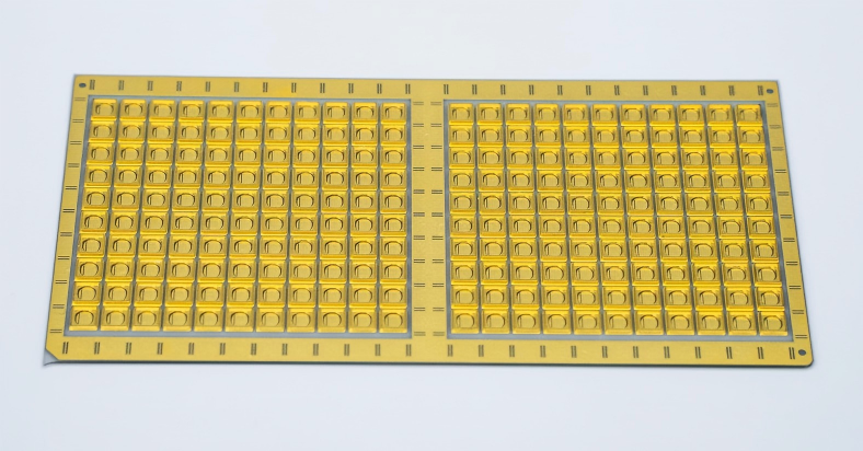

This product is a 3.9mm x 3.9mm 3D Aluminum Nitride (AlN) ceramic packaging substrate specifically designed for UVA LED chips utilizing a frontside mounting structure. It combines the high-precision circuitry of the Direct Plated Copper (DPC) process with an integrated dam structure, providing exceptional thermal management, robust chip support, and precise phosphor demarcation for traditional UVA LEDs requiring wire bonding. This substrate is an ideal choice for achieving high-reliability, mid-to-high-power UVA light sources.
Core Material: Uses high thermal conductivity (170-200 W/mK) Aluminum Nitride (AlN) to rapidly draw heat away from the chip's active layer through the substrate itself, effectively lowering the junction temperature, slowing lumen depreciation, and extending lifespan.
Efficient Thermal Path: Provides an excellent thermal foundation for the die-attach area, compensating for the longer thermal path inherent in frontside structures.
Stable Pads: The DPC process creates copper pads with strong adhesion to the ceramic substrate and a flat surface, ideal for chip eutectic bonding or silver sintering, and ensures the robustness of gold wire bond points.
Integrated Dam: The 3D dam provides a precise cavity for phosphor coating, ensuring uniform light output and effectively preventing silicone overflow from contaminating the bonding pads and wires.
Double-Layer Circuit: The 2-layer design facilitates the separation of power and ground lines, offers more flexible routing, and helps reduce parasitic parameters, enhancing electrical performance.
Environmental Resistance: The ceramic material is resistant to UV aging and high-temperature oxidation, ensuring long-term stability under UVA radiation and high-temperature conditions.
The closely matched CTE between AlN ceramic and the semiconductor chip minimizes thermal stress at the interface, improving reliability during temperature cycling.
This substrate is suitable for various UVA emission devices using frontside chip structures:
Mid-to-High Power UV Curing Modules: For curing equipment of inks, adhesives, and coatings.
Phototherapy Devices: UVA treatment modules in the medical and aesthetic fields.
Mosquito Traps: As the core UVA light source for insect attraction.
Industrial Inspection & Analysis: UVA excitation light sources for fluorescence analysis.
Resin 3D Printing: As a light source component for VAT polymerization printers.
Q1: Why choose an expensive AlN ceramic substrate over metal or FR4 for frontside UVA LEDs?
A1: Metal Core PCBs have high thermal resistance in the insulating layer, and FR4 has poor temperature resistance and thermal conductivity. UVA LEDs, especially mid-to-high-power ones, generate significant heat. The extremely low thermal resistance of AlN ceramic directly pulls heat from beneath the chip, fundamentally solving the thermal bottleneck, which is key to ensuring stable light output and device longevity.
Q2: How does this substrate improve upon the inherent thermal weakness of the frontside structure?
A2: Heat from a frontside chip is primarily dissipated through the die-attach material below it. This substrate optimizes cooling in two ways:
1. Using ultra-high thermal conductivity AlN material to maximize the efficiency of this primary path.
2. The large-area, highly conductive copper pads formed by DPC also aid in lateral heat spreading.
Q3: What is the importance of the dam structure for frontside UVA LEDs?
A3: It is crucial. The electrical connection of a frontside LED relies on surface pads and gold wires. The dam strictly confines the phosphor gel/encapsulant to the area above the chip, preventing it from flowing over the pads or stressing the wires, thereby avoiding failures caused by short circuits or wire deformation, ensuring yield and reliability.
Q4: Which die-attach method is recommended for this substrate?
A4: We highly recommend eutectic bonding or silver sintering. These methods significantly reduce the interfacial thermal resistance between the chip and substrate, fully leveraging the thermal advantage of AlN ceramic. It is also compatible with high-thermal-conductivity silver paste.
Q5: Can the pad size and dam shape be customized?
A5: Yes. The DPC process offers high design flexibility. We can customize the circuit layout and the dimensions/shape of the dam according to your specific chip size, pad layout, and optical requirements.


