


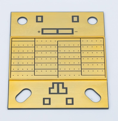

This product is a large-format 3D Aluminum Nitride ceramic packaging substrate specifically designed for high-power UVA curing systems. Utilizing advanced DPC technology and an integrated dam structure, it enables multi-chip high-density integration and precise optical control within a 35×45mm substrate area. The product combines the exceptional thermal conductivity of AlN with the circuit precision of the DPC process, providing an ideal thermal management and optical distribution solution for high-power UVA curing modules.
High thermal conductivity AlN ceramic (170-200 W/mK)
Effectively addresses thermal challenges in high-power multi-chip integration
Ensures stable junction temperature and extended service life
DPC process enables fine circuitry (line width/space down to 50μm)
Supports high-density array arrangement of dozens of UVA chips
Ensures positional accuracy and electrical connection reliability
Monolithic dam design enables precise phosphor gel control
Prevents overflow, ensuring flat and consistent light-emitting surface
Customizable dam height and shape according to optical requirements
CTE-matched ceramic and chip materials
Excellent UV resistance performance
Suitable for long-term high-temperature operation
Industrial-grade UV curing equipment
PCB solder mask curing
High-speed metal coating curing lines
Automotive component adhesive curing
Large-scale 3D printing systems
Roll-to-roll continuous curing production lines
Q1: How is flatness ensured for such large ceramic substrates?
A1: We employ special sintering processes and precision grinding technology to ensure overall substrate flatness ≤0.1%, providing an ideal mounting surface for multi-chip eutectic bonding.
Q2: What's the maximum number of chips supported?
A2: Within the 35×45mm size, typically 20-50 chips in array arrangement, depending on chip size and routing requirements. Specific quantity should be determined according to customer's optical design.
Q3: Are there standard dam height specifications?
A3: We offer three standard dam heights: 0.5mm, 0.8mm, and 1.0mm, while also supporting custom height specifications.
Q4: Does the substrate support partitioned circuit design?
A4: Yes, the double-layer design supports independent zone control, enabling separate driving of different areas to meet complex lighting requirements.
Q5: What is the maximum power density capability?
A5: With forced cooling, the substrate can withstand power density exceeding 200W/cm², fully meeting industrial high-power curing requirements.


