


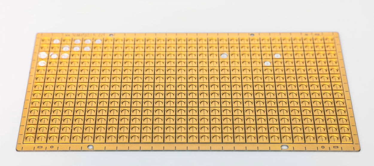

This product is a flip-chip packaging substrate specifically designed for high-power UVA LEDs. Utilizing a 3.5×3.5mm aluminum nitride ceramic substrate with advanced DPC process and dam structure, it offers excellent thermal performance and reliable structural design. It provides an ideal thermal solution and precise optical control for flip-chip applications, particularly suitable for high-power-density UVA scenarios.
AlN substrate with ≥180 W/mK thermal conductivity
Flip-chip structure achieves shortest thermal path
Supports 3-5W single chip power output
DPC integrated dam, height accuracy ±0.02mm
Effective control of phosphor thickness and profile
Prevents overflow, ensures optical consistency
Pad flatness ≤1μm
Supports solder paste printing and eutectic bonding
Pad dimensional accuracy ±5μm
Thermal cycling performance: -40℃~125℃≥1000 cycles
Excellent UV aging resistance
Service life >50,000 hours
High-power UVA curing equipment
UV disinfection modules
Photopolymerization systems
Industrial printing curing
3D printing curing systems
Medical UV therapy equipment
Q1: What are the advantages compared to front-side structure?
A1: Flip-chip structure provides shorter thermal path through direct chip attachment, improving thermal performance by about 30%, more suitable for high-power applications.
Q2: What is the height tolerance of the dam?
A2: Dam height tolerance is controlled within ±0.02mm, ensuring precise phosphor thickness control.
Q3: Can the substrate support eutectic bonding process?
A3: Yes, the product is optimized for eutectic bonding, with pad surface coating providing excellent solderability.
Q4: What is the maximum power density it can withstand?
A4: With proper heat dissipation, it can support up to 8W/mm² power density.
Q5: Do you provide optical simulation support?
A5: We can provide optical simulation analysis of the dam structure to help customers optimize optical design.


