


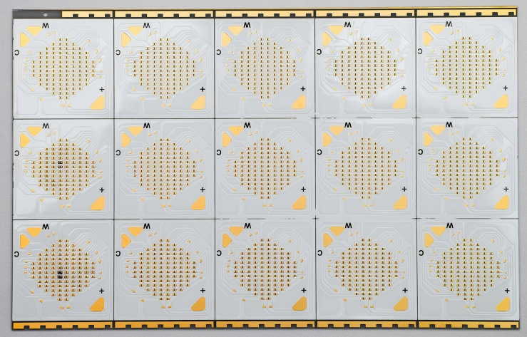

12×12mm DPC Aluminum Nitride Ceramic Substrate - For COB Packaging Lighting
This product is a high-performance ceramic substrate specifically designed for COB packaging lighting. Using high thermal conductivity aluminum nitride ceramic material and Direct Plated Copper technology, it achieves precise double-layer circuit structure within a 12×12mm square area. The product offers excellent thermal management capability, uniform current distribution and stable optical characteristics, providing an ideal integration platform for high power density LED chip arrays.
Thermal conductivity: ≥180 W/(m·K)
Thermal resistance: <1.5 K/W
Maximum power capacity: 60W
Symmetrical circuit design
Voltage drop: <0.1V
Supports multi-chip parallel connection
Chip layout accuracy: ±15μm
Pad flatness: ≤5μm
Gold layer thickness: 0.05-0.2μm
Passes 3000h 85℃/85%RH test
Thermal cycle life: -40℃~150℃>1000 cycles
Excellent UV aging resistance
Commercial lighting COB light sources
Industrial high bay lighting
Studio professional lighting
Architectural landscape lighting
Plant growth lighting
Medical special lighting
Q: Why choose AlN ceramic substrate for COB packaging?
A: COB packaging has high power density and significant heat generation. AlN's excellent thermal conductivity ensures chip junction temperature remains within safe range.
Q: How to ensure color consistency of multi-chips?
A: Precise circuit design and uniform thermal field distribution ensure all chips operate at same temperature environment.
Q: Support customized chip layout?
A: Supports different arrangement schemes according to optical design requirements.
Q: Maximum number of integrated chips?
A: Up to 100 chips on 12×12mm area, depending on chip size and optical requirements.
Q: Mass production yield?
A: Automated production line ensures product yield over 99.2% with stable quality.


