

Views: 0 Author: Site Editor Publish Time: 2026-09-30 Origin: Site


The evolution of minimally invasive surgery relies heavily on ultra-bright, ultra-compact medical endoscopes. Surgeons need high-definition, real-time visualization of internal cavities to perform complex procedures safely. The industry is rapidly shifting from bulky fiber-optic light guides to advanced chip-on-tip architectures. High-power micro-LEDs and laser diodes are now integrated directly into the distal tip of the device.
This architectural leap introduces a brutal engineering dilemma. These powerful light sources generate massive amounts of concentrated heat within a highly confined space. We are talking about diameters ranging from a mere 3mm to 10mm. Traditional FR4 printed circuit boards, and even standard metal core printed circuit boards, consistently fail under these extreme thermal loads. Inadequate heat dissipation inevitably leads to rapid component degradation, dangerous spikes in tip temperature, and potentially catastrophic failure mid-surgery.
To overcome these persistent thermal bottlenecks, hardware engineers are turning to inorganic materials. Specifically, adopting an advanced endoscope LED substrate has become a strict requirement. This guide explores the technical imperatives behind this shift, focusing on Aluminum Nitride for unmatched thermal management and the Direct Plated Copper process for micron-level manufacturing precision.
Thermal Supremacy: Aluminum Nitride delivers up to ten times the thermal conductivity of standard alumina. It is the mathematically and practically ideal foundation for high-power medical lighting.
Micron-Level Precision: The Direct Plated Copper fabrication process enables ultra-fine circuit traces and perfectly planar surfaces. These are mandatory requirements for micro-LED flip-chip bonding.
Reliability in Surgery: A proper inorganic substrate prevents heat-induced degradation. This ensures stable tissue illumination and patient safety during prolonged operations.
Optimized Manufacturing: Understanding the material science allows engineers to design highly efficient, miniaturized lighting modules while avoiding standard manufacturing limitations.
Looking at recent market intelligence, there is a definitive industry shift toward advanced inorganic substrates in the medical sector. As global demand for 4K, 8K, and 3D endoscopic imaging surges, the illumination requirements have skyrocketed. More pixels demand more light. Industry analyses indicate a massive increase in research and development investments dedicated specifically to chip-on-tip thermal management. Manufacturers are rapidly phasing out legacy materials. They must meet stringent FDA and CE thermal safety standards, which strictly cap the maximum allowable temperature of any device touching human tissue.
When you pack high-power micro-LEDs into a tiny surgical tube, physics is unforgiving. While these diodes are highly efficient at converting electricity into light, a significant percentage of the input energy still turns into heat. Because endoscope LEDs are heavily miniaturized, the power density is exceptionally high. The heat generated at the semiconductor junction must be evacuated immediately to prevent thermal runaway.
Standard FR4 materials possess a thermal conductivity of approximately 0.3 to 0.4 W/m·K. They act more like thermal insulators than conductors. When you mount high-power LEDs on FR4, the heat remains trapped at the junction. Metal core printed circuit boards offer a slight improvement by utilizing an aluminum or copper base. However, they require an organic dielectric layer to electrically isolate the copper traces from the metal core. This epoxy-based dielectric layer typically maxes out at 1 to 3 W/m·K. It creates a severe thermal bottleneck directly beneath the LED. In the constrained, sealed environment of an endoscope tip, active cooling mechanisms like fans are impossible. This bottleneck is entirely unacceptable.
In the high-stakes environment of medical diagnostics and surgery, color accuracy is a strict clinical requirement. Surgeons rely on subtle variations in tissue color to differentiate between healthy tissue, dense vasculature, and malignant growths.
When an LED operates above its optimal junction temperature, its emission spectrum actively shifts. This thermal degradation causes noticeable color shifting. The white light often pushes toward a bluish or yellowish hue, drastically reducing the Color Rendering Index. Consequently, surgical accuracy is compromised. Prolonged thermal stress also accelerates the degradation of the LED phosphor coating and semiconductor lattice. This drastically reduces the overall lifespan of a costly medical device. To pull heat away from the die instantly and maintain a stable junction temperature, integrating a reliable high thermal conductivity PCB is an absolute structural necessity.
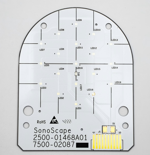
A ceramic printed circuit board utilizes advanced inorganic materials as the base substrate. Because ceramics possess highly ordered crystalline structures, they offer incredibly efficient pathways for phonon transport. They transfer heat rapidly while remaining excellent electrical insulators. Crucially, they completely eliminate the need for the thermally resistive dielectric layer found in traditional metal boards.
The fabrication process for these specialized boards involves highly controlled steps. It begins with the preparation of the bare ceramic substrate, typically sintered at extreme temperatures. Next, a metallization process deposits a conductive copper layer directly onto the ceramic. The copper is then etched or plated to form precise circuit patterns. Finally, a surface finish is applied to protect the exposed copper and provide a reliable pad for semiconductor soldering.
To make an informed engineering decision, we must look at the raw data. Below is a practical comparison of common substrate materials used in lighting modules.
| Material | Thermal Conductivity | Dielectric Layer Required? | Best Application |
|---|---|---|---|
| FR4 | 0.3 - 0.4 W/m·K | Yes | Low-power indicators |
| Metal Core PCB | 1.0 - 3.0 W/m·K | Yes | External surgical lights |
| Alumina | 24 - 30 W/m·K | No | Mid-power medical sensors |
| Aluminum Nitride | 170 - 230 W/m·K | No | High-power endoscope LEDs |
When specifying a substrate for an endoscope tip, you must evaluate the thermal resistance network of the entire assembly. While standard alumina is a vast improvement over FR4, its thermal conductivity often falls short for tightly packed micro-LED arrays driven at high currents.
In stark contrast, an AlN ceramic PCB delivers an astonishing thermal conductivity ranging from 170 to 230 W/m·K. This performance rivals that of solid metallic aluminum, but without the inherent flaw of a thermally resistive dielectric layer. This nearly tenfold increase over alumina allows the substrate to act as a near-perfect heat sink.
Beyond raw heat transfer, the coefficient of thermal expansion plays a critical role in long-term reliability. Silicon and Gallium Nitride form the core materials of modern LEDs. They exhibit a very low expansion rate, around 3 to 4 ppm per degree Celsius. Aluminum Nitride boasts a matching expansion rate of approximately 4.5 ppm per degree Celsius.
If a substrate expands at a drastically different rate than the LED during rapid heating and cooling cycles in the operating room, the resulting mechanical stress will shear the microscopic solder joints. By closely matching the semiconductor die, Aluminum Nitride entirely prevents this thermo-mechanical fatigue. Additionally, the material provides exceptional dielectric strength. This guarantees zero leakage current from the high-power lighting circuit to the exterior stainless-steel surgical casing, ensuring strict compliance with patient safety standards.
Having the right base material is only half the engineering equation. To wire multiple micro-LEDs within a 4mm diameter space, engineers require a metallization process capable of extreme precision. Older methods melt thick copper sheets onto the ceramic. That works for heavy industrial power but fails completely at producing fine trace lines due to severe etching undercut.
The Direct Plated Copper process solves this by utilizing advanced thin-film technology. During fabrication, the bare ceramic substrate is placed in a vacuum chamber. A titanium adhesion layer is sputtered onto the surface via physical vapor deposition, followed by a thin seed layer of copper. Once this ultra-thin conductive layer is established, standard photolithography and electroplating techniques build up the copper thickness precisely where the circuit traces are needed. Finally, the photoresist is stripped and the seed layer etched away.
Integrating a DPC ceramic circuit board is non-negotiable for modern endoscope design for two primary reasons.
First, it allows for ultra-fine traces. Because the process relies on additive electroplating rather than subtractive heavy etching, it achieves incredibly tight tolerances. Line widths and spaces can be manufactured as small as 50μm. This density is essential for routing complex, multi-channel circuits for RGB or white micro-LEDs at the tip of the device.
Second, it guarantees absolute surface flatness. High-power LEDs in medical devices are typically mounted using flip-chip packaging or eutectic bonding to maximize heat transfer. These advanced packaging methods require a highly planar surface to prevent voiding in the solder joint. The thin-film process results in an exceptionally flat copper surface without the crowned edges often seen in thick-film printing.
When hardware engineers combine the ultimate heat conductor with the ultimate precision plating technique, the resulting precision ceramic PCB exhibits zero thermal bottlenecks. The copper traces are intimately bonded to the base substrate at a molecular level via the vacuum-sputtered titanium layer. This entirely eliminates microscopic air gaps or thermal resistance at the interface.
The resulting board offers high-density routing capabilities without sacrificing structural integrity. Engineers can place components closer together and drive higher currents through the LEDs without exceeding safe operating temperatures.
To illustrate this impact on the bench, consider a generalized engineering scenario involving a 5mm laparoscope. By upgrading a legacy metal core light engine to an advanced inorganic board, engineering teams typically observe a massive performance leap. The superior thermal extraction allows the LEDs to be driven at a higher forward current safely. This frequently results in a 20 to 30 percent increase in lumen output.
Simultaneously, the efficient heat dissipation to the endoscope outer heat sink keeps the distal tip temperature strictly below the FDA-mandated 41 degrees Celsius safety threshold for tissue contact. Surgeons can see deeper into the surgical cavity with greater clarity, preventing tissue damage and ensuring prolonged operational stability.
While thin-film technology can achieve microscopic 50μm trace widths, high-current medical LEDs require careful electrical planning. Signal traces can comfortably be designed at 50μm to 75μm to save valuable real estate. However, power traces must be calculated based on the forward current to avoid resistive heating within the copper itself.
For a 1A LED, a trace width of at least 0.3mm to 0.5mm is highly recommended, assuming a standard 35μm copper thickness. Maintaining a minimum of 75μm spacing between high-voltage lines is also advised to prevent dielectric breakdown in dense layouts.
To move heat efficiently from the top component layer to a secondary heat sink or the stainless steel casing, thermal routing is critical. In advanced fabrication, laser-drilled vias are utilized. For maximum thermal transfer, these vias should be completely copper-filled. Designing a network of copper-filled thermal vias placed directly beneath the LED thermal pad channels heat rapidly through the substrate, taking full advantage of the high thermal conductivity matrix.
The choice of surface finish dictates the long-term reliability of the LED attachment. Electroless Nickel Immersion Gold provides a flat surface suitable for standard surface-mount soldering. However, for the most demanding medical endoscopes utilizing bare LED dies, Electroless Nickel Electroless Palladium Immersion Gold is excellent for gold wire bonding as it prevents nickel diffusion. For flip-chip LEDs or eutectic soldering, Immersion Silver is frequently recommended. It offers unparalleled thermal and electrical conductivity, ensuring a robust, void-free intermetallic bond.
Transitioning a medical device from the research phase to full-scale market availability requires a reliable manufacturing partner. Procurement managers must prioritize facilities that operate under strict regulatory frameworks. While standard quality management demonstrates baseline competence, ISO 13485 is the critical benchmark for medical devices. Manufacturers holding this certification have proven traceability, rigorous risk management, and process control systems tailored specifically for life-saving sectors.
Not all board houses can handle the brittle nature of advanced ceramics. You should audit potential partners for in-house vacuum sputtering capabilities. Outsourcing the physical vapor deposition step often leads to severe quality control issues and extended lead times. Furthermore, the manufacturer must possess advanced inspection equipment. This includes automated optical inspection calibrated specifically for highly reflective surfaces, and X-Ray inspection systems to verify void-free copper-filled vias.
The development cycle for medical hardware is notoriously iterative. A capable manufacturing partner must offer flexible, rapid prototyping services to support engineering test builds. More importantly, they must possess the infrastructure to scale seamlessly into volume production without altering the validated process parameters. Bridging the gap between initial design validation and mass market deployment is crucial for long-term project success.
As modern medical endoscopes become progressively smaller and more powerful, the thermal management requirements vastly exceed the capabilities of traditional organic materials. High heat damages delicate semiconductor components quickly, risking surgical precision and patient safety.
Advanced inorganic materials solve this critical engineering bottleneck. Aluminum nitride offers unmatched heat dissipation, while the direct plated copper process ensures the exact precision required for micro-LED integration. Combining these two technologies creates the ultimate circuit board foundation for medical lighting, making next-generation minimally invasive surgery possible.
Engineers and procurement teams must choose the right substrate to guarantee device safety and longevity. To upgrade your medical device designs, eliminate thermal failures, and secure reliable manufacturing, explore the high-performance solutions at XR MK PCB today. Match your specific project requirements with their proven ceramic capabilities to ensure your next product launch is a technical and commercial success.
Aluminum Nitride requires a highly complex manufacturing process. It involves the carbothermal reduction of aluminum oxide or direct nitridation of aluminum powder, followed by sintering at exceptionally high temperatures over 1800 degrees Celsius in a controlled atmosphere. While the raw material and processing costs are higher than standard alumina, the investment is easily justified by its tenfold higher thermal conductivity. This performance is absolutely mandatory for preventing thermal failure in high-power endoscope lighting.
Yes. Advanced fabrication techniques allow for the creation of stepped cavities or 3D structures within the ceramic substrate. By etching or machining a cavity to recess the micro-LEDs, engineers can effectively focus the light output, reduce light bleed, and save critical vertical space within the highly constrained endoscope tip.
The fabrication of specialized ceramic boards generally requires a longer lead time than standard FR4 due to the vacuum deposition and specialized laser routing processes involved. Typically, prototype runs take between 2 to 4 weeks. Partnering with an experienced, dedicated manufacturer can significantly streamline this timeline, ensuring faster iterations during the critical engineering phase.
It is strongly advised against using FR4 for modern high-power endoscope lighting. Even with an aggressive array of thermal vias, the core fiberglass-epoxy material simply cannot dissipate heat fast enough to handle the concentrated power density of micro-LEDs. The heat will bottleneck, leading to rapid color shifting and eventual device failure. A dedicated inorganic substrate is the only reliable choice for surgical applications.
While the Direct Plated Copper process is renowned for its ultra-thin precision, it is highly customizable. Standard applications typically use 10μm to 35μm copper for fine-pitch routing. However, for extreme high-current applications, the electroplating process can build the copper thickness up to 140μm. This flexibility allows engineers to balance the need for microscopic trace widths with the current-carrying capacity required for high-lumen lighting modules.
Surface roughness is a critical parameter for void-free soldering. Standard thick-film ceramics often have a rough, porous surface that traps air during reflow. The Direct Plated Copper process, however, utilizes a polished ceramic base combined with vacuum sputtering, resulting in a surface roughness often below 0.3μm. This ultra-smooth, planar finish is essential for the microscopic solder bumps used in flip-chip LEDs, ensuring perfect intermetallic connections and maximum thermal transfer.


