

Views: 0 Author: Site Editor Publish Time: 2026-10-17 Origin: Site


Did you know portable device failures frequently originate at the substrate level? Consumer gadgets and medical wearables continue to shrink at a rapid pace. Consequently, managing internal heat and signal stress transforms into a complex engineering puzzle. Selecting the correct MEMS sensor packaging substrate resolves this foundational vulnerability. This post explores why ceramic materials consistently outperform traditional alternatives. Ultimately, this material choice dictates the lifespan and accuracy of modern electronics.
Size and Performance: Modern portable devices demand packaging substrates offering extreme miniaturization. Engineers must achieve this without sacrificing thermal dissipation or electrical performance.
Material Showdown: FR4 organic boards are cost-effective but struggle with heat and moisture. Silicon and glass offer high precision yet prove brittle or cost-prohibitive for mass production.
The Ceramic Advantage: Alumina ceramic delivers superior thermal conductivity and excellent hermetic sealing. It also features a matched Coefficient of Thermal Expansion relative to silicon dies.
Top Recommendation: Specialized ceramic solutions deliver the optimal balance of miniaturization, durability, and long-term cost-efficiency for modern portable designs.
To make informed material decisions, engineering teams must first evaluate the foundational role of the substrate within micro-electromechanical systems. The substrate acts as an active participant in overall sensor performance, stability, and operational lifespan rather than a merely passive mounting platform.
At its core, the packaging substrate forms the physical and electrical bridge. It connects the delicate internal MEMS die with the external printed circuit board. MEMS devices contain both micro-electronic circuits and micro-mechanical structures, such as microscopic cantilevers or diaphragms. Therefore, the substrate must support complex signal routing while rigorously preserving the physical integrity of all moving parts.
Specifically, the substrate performs three critical functions that dictate the reliability of the entire module. First, it provides mechanical support. MEMS structures are inherently fragile. The substrate acts as a rigid backbone to protect the die from external physical shocks, vibrations, and mechanical stress caused by automated assembly processes. Second, it establishes electrical interconnects. It provides the conductive pathways required to route power and high-frequency data signals via wire bonding or flip-chip bumps. Engineers must achieve this with minimal insertion loss, crosstalk, or electromagnetic interference. Furthermore, working in tandem with the lid or encapsulant, the substrate forms an environmental shield. This base protects sensitive micro-structures from moisture ingress, particulate contamination, and corrosive gases.
Designing for portable electronics introduces a unique set of constraints. Hardware engineers are constantly forced to balance aggressive form-factor reductions with increasingly stringent performance metrics.
As consumer and medical devices become highly compact, the internal real estate allocated for sensor modules shrinks drastically. Substrates must support ultra-fine line widths and tight spacing. Accommodating multiple sensor dies within a single millimeter-scale package is now mandatory. Combining an accelerometer, a gyroscope, and a magnetometer into one tiny footprint pushes traditional routing capabilities to their absolute limits.
Miniaturization inherently leads to increased power density. Closely packed processing components generate localized heat. If the substrate lacks adequate thermal conductivity, this thermal energy accumulates rapidly around the MEMS die. Such temperature fluctuations cause micro-mechanical structures to expand or contract unpredictably. This phenomenon culminates in severe sensor drift, calibration errors, and reduced accuracy over time.
Recent market analyses of portable hardware reveal a massive shift toward heterogeneous integration and edge computing. As 5G connectivity and AI-driven algorithms become standard, sensors must process more data locally. This industry-wide evolution dictates that packaging substrates can no longer act as passive carriers. They must actively mitigate thermal spikes generated by adjacent edge processors. Market data indicates that materials failing to adapt to these high-power-density environments are rapidly being phased out of next-generation product roadmaps.
In addition, portable devices operate in highly unpredictable environments. A smartwatch might face corrosive human sweat, rapid temperature shifts from air-conditioned rooms to outdoor heat, and accidental physical drops. The packaging substrate must ensure strict air-tight sealing and structural stability. Materials absorbing moisture or warping under thermal cycling inevitably trigger premature device failure.
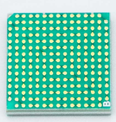
Selecting the correct material requires an objective evaluation of thermal, mechanical, and electrical properties. Below is a comparative analysis of standard materials utilized in the manufacturing sector today.
Organic laminates like FR4 and Bismaleimide Triazine resin remain common in general electronics. They are highly cost-effective and easy to manufacture in massive volumes across global supply chains. However, organic materials possess very poor thermal conductivity, typically hovering around 0.25 to 0.3 W/m·K. They also exhibit high moisture absorption rates and a mismatched Coefficient of Thermal Expansion compared to silicon MEMS dies. While suitable for low-end consumer gadgets, they pose significant reliability risks for high-precision portable sensors due to thermal warping and moisture-induced swelling.
In contrast, using silicon as a packaging substrate provides a highly integrated approach. Silicon offers a perfect thermal expansion match with the silicon MEMS die to virtually eliminate thermal stress. It allows for ultra-fine pitch routing using advanced semiconductor manufacturing techniques. Yet, silicon is inherently brittle. This fragility makes it highly susceptible to mechanical shock during drops. The manufacturing processes are also complex and expensive, which drives up the per-unit cost.
Glass is slowly emerging as an alternative for specific high-frequency radio applications. It provides exceptional high-frequency electrical properties with low signal loss. Its highly smooth surface finish suits precise thin-film metallization perfectly. Unfortunately, glass has poor thermal conductivity near 1.0 W/m·K and remains notoriously fragile. Handling glass substrates during assembly and singulation processes often results in lower production yield rates.
Ceramic materials, particularly Alumina and Aluminum Nitride, dominate high-end portable electronics today. Ceramics deliver exceptional thermal management, highly durable mechanical strength, and virtually zero moisture absorption. Historically, ceramic substrates were thicker and heavier. Modern thin-film manufacturing techniques have successfully resolved these dimensional limitations to suit miniaturized designs.
| Material Type | Thermal Conductivity W/m·K | Expansion Rate ppm/°C | Moisture Resistance | Best Application Scenario |
|---|---|---|---|---|
| FR4 Organic | ~0.3 | 14 - 17 | Poor | Low-cost consumer gadgets |
| Silicon | ~150 | 2.6 - 3.2 | Excellent | Ultra-premium zero-stress needs |
| Glass | ~1.0 | 3.0 - 8.0 | Excellent | High-frequency RF sensors |
| Alumina Ceramic | 24 - 35 | 6.5 - 7.5 | Excellent | High-reliability portable devices |
When analyzing empirical data and failure rates in portable devices, ceramic materials consistently demonstrate superior performance metrics. Their unique physical properties address the exact vulnerabilities of miniaturized sensor modules.
Alumina boasts a thermal conductivity of approximately 24 to 35 W/m·K. This rating is nearly 100 times greater than standard organic FR4. In a tightly packed smartphone or medical wearable, this allows the ceramic substrate to act as a highly efficient heat spreader. Rapidly moving thermal energy away from the sensitive MEMS die ensures stable, drift-free sensor readings even when adjacent processors operate at peak capacity.
Furthermore, the expansion rate measures how much a material swells when heated. Silicon features a low expansion rate of roughly 3 ppm/°C. Organic FR4 expands at a rate of 14 to 17 ppm/°C. When a device heats up, FR4 expands much faster than the silicon die sitting on top of it. This creates severe shear stress at the solder joints. Alumina ceramic has an expansion rate of roughly 7 ppm/°C. This matched expansion prevents mechanical stress, micro-cracking, and structural fatigue during rapid temperature fluctuations.
Portable devices increasingly rely on wireless data transmission protocols like Bluetooth, Wi-Fi, and 5G. Ceramic substrates exhibit a low dielectric constant and a very low dissipation factor. High-frequency electrical signals travel through the substrate with minimal degradation or energy loss. For wearable devices streaming real-time biometric data, this electrical stability is absolutely non-negotiable.
As portable devices continue to shrink, traditional packaging materials fail to meet the dual demands of miniaturization and thermal stability. To address these complex engineering challenges, the industry has turned to advanced ceramic manufacturing techniques. Direct Plated Copper technology applied to alumina ceramics has emerged as a highly reliable solution.
Direct Plated Copper is an advanced thin-film manufacturing process designed to bond copper metallization directly onto a ceramic base. Unlike older thick-film methods relying on high-temperature firing and glass frits, the DPC process utilizes vacuum sputtering. It deposits a thin titanium or chromium adhesion layer onto the bare alumina ceramic. Following this initial deposition, photolithography defines the exact circuit pattern, and copper is electroplated onto the exposed areas. This semiconductor-like fabrication process results in a highly precise, tightly bonded conductive layer.
The primary constraint in portable device design is available printed circuit board real estate. Because DPC utilizes photolithography rather than traditional screen printing, it allows for ultra-fine line resolution. Engineers can achieve trace widths and spacing down to 50 micrometers. When engineering a compact wearable, integrating a Mini DPC Alumina Ceramic PCB for MEMS Sensor Modules supports high-density vertical interconnect accesses and microscopic trace routing. This keeps the final module footprint incredibly small while maintaining robust thermal conductivity.
While Direct Bonded Copper has long been a staple in power electronics, it requires extremely high processing temperatures over 1000°C to form a eutectic bond. This high heat can induce thermal stress and limit the minimum thickness of the ceramic base. DPC is processed at much lower temperatures. It preserves the structural integrity of thin alumina layers, often scaling down to 0.25mm or 0.38mm thicknesses. It also provides a significantly flatter surface finish, which is critical for precise die mounting. Specifying a Mini DPC Alumina Ceramic PCB for MEMS Sensor Modules ensures top-tier electrical performance without sacrificing the structural precision required by sensitive micro-structures.
The theoretical benefits of advanced substrate materials translate into profound commercial value when applied to specific industry challenges. Substrate selection directly impacts field failure rates and warranty costs across various high-growth sectors.
Modern fitness wearables are packed with an array of sensors, including multi-axis accelerometers and biometric monitors. Imagine a runner transitioning from a freezing outdoor trail to a heated indoor gym. The wearable is subjected to constant motion, physical shocks, and exposure to corrosive sweat. An organic substrate absorbs this moisture over time, distorting delicate sensor readings. Alumina ceramic offers near-perfect hermeticity to block moisture ingress completely. Its rigid nature protects fragile internal cantilever beams from snapping under physical stress.
In the medical sector, reliability is a strict regulatory requirement. Point-of-care diagnostics, such as portable blood gas analyzers and handheld ultrasound probes, rely on MEMS sensors to deliver life-saving data. Medical sensors cannot afford baseline drift caused by thermal expansion or environmental contamination. The matched expansion rate of ceramic minimizes mechanical stress, ensuring medical devices maintain precise calibration throughout their operational lifespan.
Augmented Reality and Virtual Reality headsets process massive amounts of data in real-time to generate substantial heat. When MEMS inertial measurement units are placed near these heat sources, ambient temperature fluctuations can cause the micro-machined structures to deform slightly. This leads to tracking errors or drift in the virtual environment. By rapidly dissipating localized heat, ceramic substrates ensure stable operating temperatures for zero-latency head tracking. The small footprint enabled by a Mini DPC Alumina Ceramic PCB for MEMS Sensor Modules allows designers to pack more battery capacity into the headset by shrinking the sensor module itself.
Selecting the appropriate material architecture during the early design phase prevents costly redesigns and product recalls later. Procurement managers and hardware engineers should evaluate their specific project requirements against objective material data rather than relying on abstract concepts.
First, analyze the thermal envelope of your device. Calculate the total power dissipation of the active components located near the sensor module. As a general rule of thumb in hardware engineering, if the localized temperature is projected to fluctuate rapidly, default to a ceramic-based solution. If the sensor requires strict thermal stability to maintain accuracy, ceramic is also mandatory. The slightly higher upfront component cost is quickly offset by the elimination of thermal mitigation hardware and a drastic reduction in commercial field failures.
Next, consider the operating environment to dictate the required level of hermetic sealing. Assess whether the portable device will be exposed to high humidity, submerged in fluids, or subjected to extreme cold-to-hot transition cycles. Organic materials are hygroscopic. They absorb ambient moisture which causes short circuits in ultra-fine pitch routing. For harsh environments, alumina ceramic provides the optimal balance of rugged mechanical strength and absolute moisture resistance.
Finally, partner with a specialized substrate manufacturer. The manufacturing of advanced thin-film ceramics is a highly specialized field. Not all printed circuit board fabricators possess the cleanroom environments, vacuum sputtering equipment, or photolithography expertise required to produce high-yield boards with 50-micrometer precision. Specifying a high-grade Mini DPC Alumina Ceramic PCB for MEMS Sensor Modules from an experienced vendor ensures your design intent translates accurately into the final manufactured product. This secures the long-term reliability of your portable device.
Choosing the right material ensures your portable device succeeds in a highly competitive market. While various materials exist, the unique constraints of portable electronics quickly narrow the field. Small devices demand strict size reductions and thermal management without compromise. Ceramic options lead the modern electronics industry today because the proper packaging substrate dictates long-term sensor reliability. By upgrading your sensor modules to high-quality ceramic solutions, you provide unmatched precision, durability, and performance for your next-generation projects.
Are you ready to eliminate thermal drift and signal loss in your next portable device design? Visit https://www.xrmkpcb.com to explore advanced ceramic solutions and find the perfect substrate configuration tailored to your specific engineering requirements.
While organic materials like FR4 present the lowest initial procurement cost, they often lead to higher lifetime costs in precision applications due to thermal drift and moisture-induced failures. For portable devices requiring high reliability and accuracy, Alumina Ceramic manufactured via the DPC process offers the best long-term return on investment by significantly reducing warranty claims and field failure rates.
DPC stands for Direct Plated Copper. It is a highly precise thin-film manufacturing process. By utilizing vacuum sputtering and photolithography, DPC allows for the creation of ultra-fine copper circuits securely bonded to ceramic substrates. This technology is highly favored for miniaturized MEMS sensors because it supports high-density routing in extremely small form factors without the extreme heat required by older methods.
Standard FR4 possesses very poor thermal conductivity and expands at a significantly different rate than the silicon MEMS die. In tightly packed, heat-generating portable devices, this mismatch causes the substrate to expand and contract unevenly. Over time, this mechanical stress distorts the micro-structures within the sensor, leading to data inaccuracy or physical cracking of the die.
Sensor accuracy is highly dependent on mechanical and thermal stability. A DPC alumina ceramic board improves accuracy by providing an exceptionally flat mounting surface, which prevents initial installation stress. Furthermore, its superior heat dissipation prevents localized hot spots to ensure the sensor does not experience thermal drift. This stable physical and thermal foundation allows the MEMS micro-structures to collect precise, undistorted data.
Standard integrated circuit packaging primarily focuses on electrical connections and thermal dissipation for solid-state silicon. MEMS packaging is significantly more complex because it must protect moving mechanical parts. The substrate and encapsulant must provide a hermetic seal against moisture and particulates while ensuring zero mechanical stress is transferred to the delicate internal cantilevers or diaphragms.
Substrate thickness directly impacts both the overall footprint of the portable device and its thermal dissipation capabilities. A thinner ceramic substrate, such as a 0.25mm or 0.38mm profile achieved through the DPC process, reduces the thermal resistance path. This allows heat to escape the sensor module much faster. It prevents localized thermal buildup that causes sensor drift in highly compact wearable designs.


