

Views: 0 Author: Site Editor Publish Time: 2026-09-03 Origin: Site


A meticulously engineered sensing die holds little value if its surrounding architecture fails under pressure. Even the most advanced silicon sensing element suffers from premature failure, erratic signal drift, or manufacturing bottlenecks when the underlying foundation cannot withstand environmental stress. For B2B buyers, product managers, and engineers, early-stage product development often reveals a harsh truth. Poor material selection at the base level is the leading cause of field failures.
The packaging board emerges as the critical building block for long-term reliability. Engineering teams must view it as a structural and thermal shield rather than a mere electrical interconnect. This guide walks buyers through exactly what to verify before committing to a custom production run. We will explore advanced material selection, specific manufacturing compatibilities, and stringent quality audits.
Material Selection is Make-or-Break: The thermal and mechanical stability of the final product is dictated entirely by the base material.
MEMS Compatibility: Proper isolation and hermetic sealing are non-negotiable to prevent signal interference in sensitive micro-electromechanical systems.
Manufacturing Technologies Matter: Buyers must strictly audit a supplier's metallization techniques and via-filling capabilities for high-precision routing.
Customization Requires Rigorous DFM: A successful product launch relies on thorough Design for Manufacturability checks, iterative prototyping, and stringent QA testing before mass manufacturing.
The demand for ultra-compact, high-precision pressure sensors is surging across the automotive, aerospace, and industrial IoT sectors. Recent market analyses indicate a definitive shift away from traditional organic boards. Engineers are increasingly adopting advanced inorganic materials to meet stringent high-temperature and harsh-media requirements. As sensing elements shrink, the packaging must handle higher power densities and tighter routing tolerances. This evolution forces manufacturers to innovate rapidly, making the choice of a robust foundation more critical than ever.
The foundational framework of any pressure-sensing device serves a complex dual purpose. It must physically protect the delicate internal sensing element from corrosive elements. Simultaneously, it must allow accurate environmental pressure to reach the sensor without inducing mechanical distortion. Achieving this balance requires absolute precision.
Consider an industrial pipeline monitoring scenario. When a sensor is deployed in an environment with extreme temperature fluctuations, the materials expand and contract. If a buyer selects a substrate with a mismatched Coefficient of Thermal Expansion relative to the silicon die, it induces severe packaging stress. This mechanical strain transfers directly to the die. It mimics the effect of actual physical pressure. The result is false pressure readings, continuous calibration drift, and eventually, the physical fracturing of the sensor itself.
The right substrate acts as a fortress against external degradation. In automotive and heavy industrial applications, sensors are routinely exposed to moisture, aggressive fluids, and corrosive gases. A robust pressure sensor ceramic substrate ensures these contaminants cannot bypass the structural seals. This preserves the integrity of the internal reference cavity and extends the operational lifespan of the device.
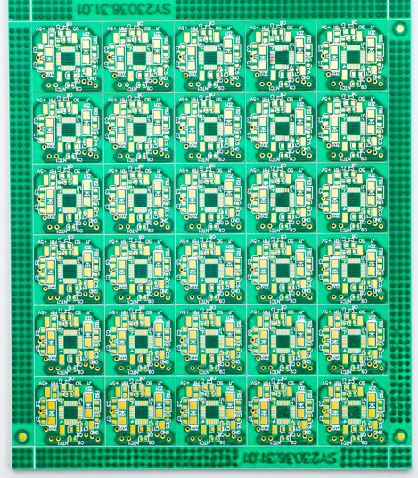
Navigating the myriad of available materials can be daunting. Aligning the physical properties of the board with the demands of the end application is paramount for success.
When operating in high-stakes environments, choosing inorganic materials is often the defining factor for reliability. Materials such as Aluminum Oxide and Aluminum Nitride are considered the gold standard in the industry. Their thermal expansion closely mirrors that of the silicon die, virtually eliminating the stress discussed earlier. Ceramics offer exceptional thermal conductivity, high mechanical rigidity, and superior chemical resistance compared to organic alternatives. For instance, a standard 96 percent alumina board provides reliable thermal conductivity around 24 W/m·K, which is vastly superior to standard FR4.
As devices shrink, traditional thick-film ceramics often fall short in routing density. This limitation has led to the rapid adoption of Direct Plated Copper technology. By utilizing physical vapor deposition followed by electroplating, manufacturers can bond a highly precise copper layer directly onto the alumina base. A DPC alumina substrate is ideal for high-density wiring and superior heat dissipation. Buyers should look for suppliers capable of achieving fine line and space resolutions down to 20 micrometers, with customizable copper thicknesses ranging from 10 to over 100 micrometers. This allows engineers to pack more functionality into miniaturized footprints without risking thermal bottlenecks.
Standard FR4 or Bismaleimide Triazine substrates are highly cost-effective and suitable for benign environments like basic consumer electronics. However, organic substrates absorb moisture and exhibit high thermal expansion. Relying on them for high-reliability sensing applications frequently results in premature field failures and costly product recalls.
Recent industry trends highlight a massive shift toward ultra-miniaturized IoT and automotive sensors, such as Tire Pressure Monitoring Systems. As these devices become smaller and more integrated, the complexity of MEMS sensor packaging increases exponentially. Micro-electromechanical systems require highly specialized structural designs to function correctly.
Engineers must ensure the layout inherently isolates the sensing die from external mounting stresses. When a technician torques a bolt or solders the final assembly into a larger system, the base board can warp. Designing specific isolation trenches or utilizing compliant die-attach materials absorbs this mechanical shock before it reaches the sensor.
Space is at an absolute premium. Buyers must verify that their chosen supplier can produce ultra-fine resolutions. Achieving trace widths below 30 micrometers on ceramic is challenging. Yet, it is a necessary capability to accommodate the shrinking footprints of next-generation chips.
Guiding the design toward the correct sealing method is crucial based on the deployment environment. For aerospace or submerged applications, true hermetic sealing is required to block all gas and moisture ingress. This is often achieved via gold-tin eutectic soldering directly onto the metallization. For less extreme environments, high-grade polymer potting may suffice, provided the surface promotes strong chemical adhesion.
Before initiating a custom manufacturing run, it is vital to align the sensor packaging board specifications with end-market realities. Different sectors enforce vastly different regulatory and performance standards.
If the device is destined for medical equipment, such as invasive blood pressure monitors, the material must withstand harsh chemical sterilization processes. Materials must be audited for biocompatibility to ensure no toxic outgassing occurs during operation.
Automotive engineers expect components to survive brutal conditions. Buyers must specify requirements for High-Temperature Operating Life and severe vibration resistance. A board used in an engine control unit must maintain absolute electrical and structural integrity even when subjected to constant 150°C heat and intense mechanical vibration.
For wearables and smart home devices, the engineering focus shifts slightly. Balancing aggressive cost targets and ultra-compact sizes with moderate reliability becomes the primary goal. Communicating these volume-driven constraints early allows the manufacturer to suggest appropriate, cost-effective material alternatives.
A meticulously engineered design holds little value if the manufacturing facility cannot execute the assembly with consistent reliability. The assembly process is highly sensitive to surface conditions, via integrity, and metallization precision. Buyers must audit the manufacturer’s specific capabilities before initiating any production run.
The physical connection between the sensing die and the base is a critical failure point. Buyers must verify that the chosen ceramic sensor PCB features surface finishes optimized for robust die attach and wire bonding. Standard organic finishes often degrade under the high temperatures required for ceramic assembly.
Engineers should look for surface finishes such as Electroless Nickel Immersion Gold or bare gold plating. These finishes prevent oxidation and provide a highly planar surface. This uniformity is essential for uniform die attachment and strong intermetallic bonding. Request empirical data on wire pull strengths and die shear testing specific to their ceramic boards. The absence of this data often indicates a lack of maturity in handling high-reliability packaging.
As devices continue to shrink, manufacturers utilize vertical space through 3D packaging. This requires high-density interconnects and through-hole vias. Creating reliable vias in hard inorganic materials is significantly more complex than in standard FR4.
Buyers must evaluate the capability to drill, plate, and fill vias without inducing micro-cracks. High-quality filled vias are critical for preventing gas or moisture leakage. Ask the supplier about their via aspect ratio limits and the specific conductive pastes used for filling. The thermal expansion of the via fill material must closely match the surrounding material to prevent delamination during thermal cycling.
High defect rates during manufacturing directly translate to increased unit costs and delayed product launches. Buyers should request historical yield data for similar custom projects rather than just theoretical capabilities.
Understanding the step-by-step yield provides a transparent view of the factory's process control. A facility utilizing rigorous Statistical Process Control and maintaining high Process Capability Index values will demonstrate consistent yield rates. This data-driven approach ensures the transition from small-batch prototyping to high-volume manufacturing remains economically viable.
| Audit Parameter | Ideal Specification | Potential Risk if Ignored |
|---|---|---|
| Surface Finish | ENIG, ENEPIG, Soft Gold | Poor wire bonding, signal loss |
| Via Fill Material | Thermally matched conductive paste | Hermetic seal failure, micro-cracking |
| Metallization Precision | ≤ 20µm line/space resolution | Inability to support miniaturized MEMS |
| Process Control | Cpk > 1.33 on critical dimensions | High batch-to-batch variability |
Engaging a manufacturer for a custom project requires a structured approach. Skipping steps in the customization roadmap frequently results in costly redesigns, delayed time-to-market, and compromised field reliability.
The customization journey must always begin with a rigorous Design for Manufacturability review. A common pitfall is creating a CAD layout that works perfectly in simulation but exceeds the physical tolerances of the manufacturing equipment.
Engineers and the factory technical team must align on critical parameters such as trace width, spacing, and panel utilization. This is the stage to verify that thermal dissipation pathways are optimized. Buyers should expect a detailed report highlighting potential bottlenecks and suggesting design modifications to improve yield.
Once the design is approved, the next mandatory step is rapid prototyping. Buyers should never proceed directly to mass production based solely on theoretical approvals. Ordering a small batch allows engineering teams to conduct physical validation testing.
Prototypes must be subjected to thermal cycling, vibration testing, and signal integrity analysis. If the device exhibits signal drift, engineers can perform failure analysis using Scanning Electron Microscopy to identify defects. This iterative loop is essential for confirming the design performs as expected under real-world conditions.
After validation, the focus shifts to volume scaling and supply chain risk management. A manufacturer may excel at producing ten pristine prototypes but struggle to maintain quality across a run of ten thousand units.
Buyers must verify equipment redundancy and automated optical inspection capabilities. Raw material sourcing is also a critical factor. Ensure the manufacturer has secured a stable supply of high-grade aluminum oxide or aluminum nitride powder. Establishing clear Service Level Agreements regarding lead times and inventory management is vital before signing a mass production contract.
The final hurdle is auditing the supplier's Quality Assurance frameworks and industry compliance standards. For devices deployed in critical applications, empirical evidence of reliability is non-negotiable.
Different industries mandate specific regulatory frameworks. The manufacturer must hold the certifications relevant to the end market.
ISO 9001: The baseline for standard industrial applications, ensuring basic quality management systems are in place.
IATF 16949: Mandatory for automotive applications. This requires strict adherence to the Production Part Approval Process, ensuring total traceability and defect prevention.
ISO 13485: Critical for medical devices. This certification ensures the manufacturer adheres to stringent risk management and lot traceability protocols.
Buyers must request valid copies of these certificates and verify the scope covers advanced inorganic manufacturing.
Certifications provide a framework, but physical reliability testing proves the product's durability. Buyers must confirm that the manufacturer conducts comprehensive in-house testing compliant with JEDEC or IPC standards.
| Test Category | Standard Protocol | Purpose |
|---|---|---|
| Thermal Shock | MIL-STD-883 | Verify thermal compatibility and prevent micro-cracking. |
| HAST | JESD22-A110 | Ensure hermeticity and resistance to moisture. |
| Shear Strength | MIL-STD-883 | Validate die attach and trace adhesion strength. |
Customizing a foundational board is a highly technical, multi-layered process. Material choices dictate the ultimate success or failure of your sensing equipment in the field. From leveraging advanced direct plated copper technology for thermal management to ensuring rigorous structural design compatibility, every decision matters.
Always verify specific capabilities, yield rates, and QA testing protocols before transitioning into mass production. Treating your manufacturer as a strategic partner bridges the gap between design theory and manufacturing reality. This collaborative approach guarantees optimal performance and long-term product durability. Visit www.xrmkpcb.com to explore high-performance ceramic boards tailored for your next-generation sensing devices, and consult with industry experts to secure a robust foundation for your custom project today.
A Direct Plated Copper alumina board is an advanced packaging solution where a highly precise copper layer is directly plated onto an aluminum oxide base using physical vapor deposition and electroplating. It merges the excellent thermal conductivity and mechanical rigidity of inorganic materials with fine-line copper routing. This precision is essential for accommodating ultra-small footprints while ensuring stable performance under fluctuating environmental conditions.
Standard FR4 organic materials possess a high thermal expansion rate, meaning they expand and contract significantly during temperature changes. This continuous thermal movement transfers mechanical stress to the sensitive die, leading to signal drift, inaccurate readings, or physical fracturing. Inorganic materials like alumina or aluminum nitride closely match the thermal expansion of silicon. This matching ensures structural stability, minimizes packaging-induced stress, and maintains accurate calibration in high-temperature environments.
The primary challenges revolve around protection without interference. Engineers must isolate the delicate mechanical structures of the die from external mounting stresses and thermal fluctuations. Achieving a reliable hermetic seal is critical to protect internal components from moisture, corrosive gases, and particulate contaminants. Managing heat dissipation is also a major hurdle, as these devices often operate in confined spaces with high power densities.
The timeline varies based on design complexity and testing requirements. The initial design review and tooling preparation take about 1 to 2 weeks. The rapid prototyping phase, which includes manufacturing the initial batch and conducting baseline physical tests, requires an additional 2 to 4 weeks. Once prototypes are approved, transitioning to mass production usually takes 4 to 8 weeks, depending on raw material availability and factory capacity.
A mismatch in the Coefficient of Thermal Expansion between the silicon sensing element and the underlying board causes the materials to expand at different rates when exposed to heat. This differential expansion creates mechanical strain on the die. Because the sensor is designed to measure physical stress, it cannot distinguish between actual environmental pressure and the stress induced by the packaging. This results in false data outputs and severe calibration drift over time.
Electroless Nickel Immersion Gold and Electroless Nickel Electroless Palladium Immersion Gold are considered the optimal surface finishes for high-reliability wire bonding. These finishes provide an extremely flat, oxidation-resistant surface that promotes strong intermetallic connections during the bonding process. Unlike standard organic solderability preservatives, these premium finishes withstand the high-temperature assembly profiles required for advanced inorganic boards without degrading.


