

Views: 0 Author: Site Editor Publish Time: 2026-09-10 Origin: Site


Are your power electronics failing under extreme thermal stress? Traditional FR4 boards frequently melt, warp, or delaminate during high-voltage operations. This thermal degradation leads to massive system failures in modern electronic devices. From an engineering standpoint, relying on standard organic materials for high-power applications is a massive risk. In this comprehensive guide, we will explore the critical engineering specifications required to prevent these catastrophic breakdowns. By examining specialized materials and precise manufacturing techniques, we will uncover how thick film integrated circuits provide the reliable foundation necessary for robust power module designs.
Superior Reliability: Thick film integrated circuits offer enhanced durability in harsh environments. They vastly outperform standard epoxy-glass boards under severe thermal and mechanical stress.
Voltage Specifications: Utilizing an inorganic ceramic base provides exceptional dielectric strength. This effectively prevents electrical breakdown and carbon tracking in high-power applications.
Current Specifications: Customizable trace thicknesses allow for massive current-carrying capacities. The substrate acts as an immediate heat sink to maintain safe operating temperatures.
Thermal Specifications: An alumina ceramic base delivers excellent thermal conductivity ranging from 24 to 28 W/m·K. It also provides precise thermal expansion matching to protect delicate semiconductor dies.
Thick vs. Thin Film: Thick film remains the definitively preferred engineering choice for high-power modules. Its physical robustness and cost-effectiveness at scale are unmatched in heavy-duty applications.
Understanding the baseline technology is essential before evaluating specific electrical and thermal parameters. In the realm of power electronics, component failure is frequently linked directly to substrate limitations. Thick film technology addresses these fundamental material constraints head-on. It offers a ruggedized platform built specifically for extreme conditions.
Manufacturing these circuits requires a highly controlled screen-printing and firing process. In practice, engineers utilize fine-mesh stainless steel screens ranging from 200 to 325 mesh. These screens deposit specially formulated pastes onto a bare ceramic base. The thixotropic pastes include conductive materials like silver, palladium, or gold. They also contain dielectric insulators and resistive ruthenium-based compounds.
Once the initial printing is complete, the substrate undergoes a controlled drying phase at approximately 150°C. This step evaporates the organic solvents. The critical transformation occurs during the firing process in a multi-zone conveyor furnace. The circuits are subjected to peak temperatures around 850°C for about 10 minutes. This high-temperature sintering melts the glass frit within the paste. It permanently fuses the electrical traces and passive components to the ceramic matrix. This additive manufacturing approach allows multiple layers of conductors and insulators to be stacked. The result is a highly dense and mechanically robust circuit capable of surviving intense mechanical shocks.
Looking at current industry trajectories, a significant paradigm shift is underway. Recent market analyses highlight the rapid adoption of wide-bandgap semiconductors like Silicon Carbide and Gallium Nitride. These advanced components are pushing power densities to unprecedented levels. Because these advanced dies operate efficiently at much higher junction temperatures, the thermal bottleneck has shifted entirely. The limitation is no longer the silicon itself, but rather the packaging materials. Consequently, engineers are aggressively phasing out the traditional power module PCB in favor of ceramic-based hybrid circuits.
Standard FR4 boards have a glass transition temperature hovering around 130°C to 150°C. When power modules exceed these thresholds, the organic resins degrade rapidly. Thick film technology entirely eliminates this bottleneck. By utilizing an inorganic ceramic base, these modules can safely operate at continuous temperatures exceeding 150°C. Specialized iterations can even handle up to 200°C. Printing heavy-duty resistors and capacitors directly onto the substrate drastically reduces the physical footprint of the module. This direct integration eliminates the need for bulky surface-mount soldered resistors. It reduces parasitic inductance and minimizes vulnerable solder joints, which directly correlates to a significantly higher field reliability.
Designing traction inverters, grid-tied power supplies, and industrial motor drives requires strict adherence to voltage safety margins. In these high-stress scenarios, thick film technology provides distinct and measurable advantages in high-voltage isolation.
The primary defense against catastrophic electrical arcing in a high voltage ceramic circuit is its inherent dielectric strength. This metric defines the ability of a material to withstand high electrical fields without experiencing a conductive breakdown. In thick film architectures, multiple layers of specialized glass-ceramic dielectric pastes are printed and fired systematically between the conductive layers.
Standard thick film dielectric layers exhibit a remarkable breakdown voltage exceeding 10 kV/mm. When combined with the insulating properties of the underlying ceramic base, the total circuit assembly can safely isolate thousands of volts. The ceramic itself often surpasses 15 kV/mm independently. This level of isolation is an absolute necessity for engineers designing Insulated-Gate Bipolar Transistor modules or high-voltage direct current converters. During production testing, these circuits survive rigorous high potential testing without issue. They contain no organic resins capable of carbonizing into conductive paths under stress. Therefore, the dielectric layers maintain their integrity even during severe transient voltage spikes.
Operating voltage limits are not dictated solely by material breakdown. The physical layout of the board plays an equally critical role. Creepage and clearance must strictly adhere to international safety standards to prevent surface tracking. Creepage is the shortest path between two conductive parts along the surface, while clearance is the shortest distance through the air.
Thick film screen printing offers exceptional dimensional stability. Etched copper on a standard board frequently suffers from chemical undercutting and rough edges. In contrast, printed thick film traces boast smooth and highly predictable boundaries. This manufacturing precision allows engineers to calculate and implement aggressive trace spacing with absolute confidence. Specialized insulating overglazes are often printed over high-voltage traces to further enhance reliability. This protective layer acts as a physical barrier against environmental contaminants. It prevents moisture, dust, or potting compound outgassing from reducing the effective creepage distance.
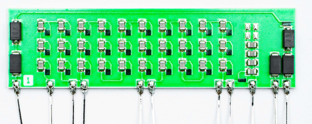
Power modules are tasked with managing massive electrical loads without experiencing thermal runaway or trace vaporization. The current-carrying capacity of a circuit is tethered directly to its conductor geometry and the ability of the substrate to pull heat away from the active traces.
Standard copper-clad boards rely primarily on the width and thickness of the copper foil to carry current. Thick film takes a markedly different approach. The printed conductive pastes are typically thinner per individual layer, usually measuring 10 to 15 microns. However, their actual current density limits are remarkably high.
This impressive current density is achieved through two distinct mechanisms. First, the screen-printing process facilitates the selective buildup of conductive layers. Engineers can program multiple print passes on specific high-current nets to dramatically increase the cross-sectional area where it matters most. Second, the underlying ceramic substrate acts as an immediate and highly efficient heat sink. The ceramic pulls thermal energy away from the conductive trace exponentially faster than standard epoxy-glass. As a result, the trace remains significantly cooler under heavy loads. This superior thermal efficiency dictates that a thick film trace can carry substantially more amperes per square millimeter without risking a burnout.
Managing inrush surge currents and continuous high-power loads requires incredibly robust resistive elements. In advanced designs, resistive pastes are printed directly onto the power resistor substrate. This allows them to be scaled in size and geometry to handle massive energy dissipation that would instantly destroy standard surface-mount resistors.
These printed resistors offer a highly versatile range of sheet resistances. They typically span from 1 ohm per square up to 10 megaohms per square. Engineers can dial in specific resistance values tailored exactly to the power-handling requirements of the module by mathematically adjusting the length-to-width ratio of the printed layout. These printed resistors undergo active laser trimming to ensure precise current control. An automated laser system cuts a microscopic notch into the fired resistor material. It gradually raises the resistance until it hits a strict tolerance level, often ±1 percent or better. This powerful combination of heavy-duty thermal dissipation and tight electrical tolerance makes the ceramic resistor substrate indispensable for current-sensing shunts.
Thermal fatigue remains the leading cause of power module breakdown in the field. Semiconductor dies continue to shrink while their power outputs increase. Managing localized heat density has become the primary engineering challenge of the decade.
To truly understand the thermal advantages of ceramic materials, we must look at the raw data. Below is a core comparison of substrate materials commonly evaluated for power electronics.
| Substrate Material | Thermal Conductivity | Thermal Expansion Coefficient | Primary Use Case |
|---|---|---|---|
| Standard FR4 Epoxy | 0.3 to 0.4 W/m·K | 14 to 17 ppm/°C | Low-power consumer electronics |
| 96% Alumina Ceramic | 24 to 28 W/m·K | 7.0 ppm/°C | Industrial power modules, EV inverters |
| Aluminum Nitride | 170 to 200 W/m·K | 4.5 ppm/°C | Ultra-high power density aerospace modules |
The undisputed industry standard for thick film applications is the alumina ceramic substrate, typically utilized at 96 percent purity. The defining technical advantage of alumina is its exceptional thermal conductivity. As shown in the table above, standard printed circuit boards offer a dismal thermal conductivity. In stark contrast, 96 percent alumina delivers a thermal conductivity ranging from 24 to 28 W/m·K.
This metric means an alumina substrate transfers heat nearly 80 times more efficiently than standard organic materials. When a high-power silicon carbide die generates intense heat, the alumina substrate rapidly conducts that thermal energy away from the junction. It spreads the heat evenly across the surface or transfers it directly into an attached aluminum heat sink. This rapid thermal dissipation prevents localized hotspots from forming beneath the dies. Actively maintaining lower junction temperatures increases the overall switching efficiency of the power module and significantly extends the operational lifespan of the active components.
Thermal conductivity is only half of the thermal management equation. Mechanical stability during rapid temperature fluctuations is the other crucial factor. Power modules cycle on and off constantly. Materials naturally expand when heated and contract when cooled. This physical property is measured by the Coefficient of Thermal Expansion.
Silicon semiconductor dies possess an expansion coefficient of approximately 3 ppm/°C. Standard FR4 expands at a highly mismatched rate of 14 to 17 ppm/°C. This severe physical mismatch generates immense mechanical shear stress on the solder joints connecting the die to the board. It inevitably leads to solder fatigue, micro-cracking, and sudden module failure. Fortunately, alumina ceramic bridges this gap with a coefficient of approximately 7 ppm/°C. This closer match drastically reduces the shear stress exerted on delicate wire bonds during rapid thermal cycling.
When engineering high-reliability power electronics, technical decision-makers frequently evaluate both thick film and thin film technologies. Their manufacturing methods, physical properties, and optimal use cases differ entirely. Let us break down how to choose the right architecture for your project.
Thin film circuits are manufactured utilizing vacuum deposition processes like sputtering. This creates an extremely uniform and microscopic layer of material, typically between 0.1 to 1.0 micrometers thick. Thin film excels in applications requiring ultra-low electrical noise. However, this microscopic thinness becomes a severe liability in power electronics. Thin films simply lack the physical mass required to absorb large transient thermal loads without vaporizing.
Thick film circuits are manufactured using screen-printing. The resulting fired layers are substantially thicker, usually ranging from 10 to 50 micrometers. This added physical mass gives thick film technology a massive advantage in power handling. The robust printed traces easily withstand severe voltage spikes and heavy continuous currents. For power modules, thick film is the empirically proven choice.
Procurement managers must evaluate unit economics alongside raw electrical specifications. Thin film manufacturing requires highly expensive vacuum chambers and stringent cleanroom environments. It is a high-cost process reserved for specialized aerospace sensors or high-frequency RF applications.
Thick film manufacturing operates at standard atmospheric pressure. The screen-printing methodology facilitates rapid production lines. Multiple circuits can be printed, dried, and fired in high-throughput conveyor systems simultaneously. The ability to print passive components directly onto the substrate eliminates the need to purchase and solder discrete surface-mount components. This reduces both the bill of materials and assembly time. For mass-producing rugged industrial modules, thick film delivers vastly superior economies of scale.
The theoretical advantages of high voltage isolation, heavy current capacity, and superior thermal management translate directly into measurable performance gains in the field. Standard boards are being rapidly replaced by ceramic-based solutions across multiple heavy industries.
The aggressive electrification of the automotive industry has pushed power electronics to their physical limits. The current trend of moving to 800V architectures means electric vehicle traction inverters must process hundreds of amps safely. Furthermore, these modules are subjected to constant mechanical vibration and extreme under-hood temperatures.
A thick film ceramic circuit is uniquely qualified to survive this harsh environment. The matched thermal expansion of the ceramic prevents solder joints from fracturing during daily driving. Additionally, the high thermal conductivity of the substrate allows automotive engineers to design significantly smaller liquid-cooling systems. This directly contributes to overall vehicle efficiency and extended driving ranges.
Solar and wind inverters are expected to operate continuously for decades with zero maintenance. These massive systems convert highly variable DC power into stable AC power for the electrical grid. A standard circuit board is highly susceptible to dielectric breakdown over time when exposed to sustained high voltages up to 1500V.
Deploying high voltage ceramic circuits allows inverter manufacturers to benefit from the inherent dielectric strength of the ceramic material. The ability to print robust resistors directly onto the substrate allows these industrial power supplies to safely absorb massive transient energy spikes from grid fluctuations. This prevents catastrophic system failures and ensures uninterrupted power delivery.
Designing power modules requires mastering complex thermal and electrical specifications. Standard boards often fail under heavy stress. Upgrading to reliable materials for harsh environments is a necessity. Thick film circuits on ceramic substrates decisively solve these issues by offering excellent heat management and unparalleled high voltage isolation. If you are dealing with thermal runaway or dielectric breakdown in your current designs, it is time to evaluate a ceramic upgrade.
Ready to upgrade your power modules? Explore robust, high-performance ceramic solutions tailored to your specific voltage, current, and thermal needs. Visit XRMKPCB to find the exact thick film integrated circuit specifications required to ensure long-term durability and field reliability for your next engineering project.
Thick film circuits built on ceramic substrates typically support continuous operating temperatures ranging from 150°C to 200°C. This depends heavily on the specific conductor pastes and solders applied during assembly. This thermal ceiling far exceeds the capabilities of standard FR4 materials, which generally begin to degrade structurally and delaminate above 130°C.
Yes, absolutely. In applications characterized by extreme thermal cycling, heavy current loads, or strict space constraints, replacing a standard FR4 board with a thick film ceramic solution is highly recommended. The ceramic alternative provides vastly superior thermal conductivity and allows for the direct integration of passive components, ultimately reducing the overall physical footprint of the module.
Alumina serves as the industry standard because it offers an highly proven balance of engineering properties and cost-effectiveness. It provides exceptional electrical insulation, high mechanical rigidity, and a thermal conductivity ranging from 24 to 28 W/m·K. This is significantly higher than traditional organic materials, making it ideal for rapid heat dissipation.
A power resistor substrate is manufactured entirely from inorganic ceramic materials rather than layers of epoxy-resin and woven fiberglass. This fundamental structural difference allows engineered resistive pastes to be screen-printed and fired directly onto the surface at extreme temperatures. Consequently, the substrate itself acts as a massive heat sink, allowing the printed resistors to safely dissipate high-wattage thermal energy without burning or delaminating.
In thick film manufacturing, the fired conductive layers typically range from 10 to 15 microns per printed pass. However, engineers can specify multiple print passes to build up the thickness to 50 microns or more for high-current applications. This added physical mass is what gives thick film its superior surge current handling capabilities.
Advanced wide-bandgap devices generate highly concentrated heat loads. A ceramic substrate rapidly pulls this heat away from the semiconductor junction due to its high thermal conductivity. Furthermore, the ceramic's coefficient of thermal expansion closely matches the silicon die. This prevents the solder joints from cracking under the mechanical stress of constant heating and cooling, thereby extending the operational lifespan of the entire module.


