

Views: 0 Author: Site Editor Publish Time: 2026-10-24 Origin: Site


As engineers, we know that managing extreme heat in modern power electronics is the ultimate bottleneck. You cannot treat thermal management as an afterthought. With the rapid adoption of Silicon Carbide and Gallium Nitride devices, design teams frequently face a pivotal crossroads. We must select the absolute optimal ceramic metallization process to prevent premature module failure.
Direct Bonded Copper serves as the traditional heavyweight for brute-force current. However, thick film technology presents distinct structural and economic advantages. These benefits frequently make it the superior option for highly integrated module designs. This comprehensive guide breaks down the technical nuances, cost implications, and exact scenarios where a Thick Film Ceramic Circuit Board for Power Modules outshines Direct Bonded Copper. By understanding these core differences, your engineering and procurement teams can make highly cost-effective design decisions.
Key Takeaways
Design Flexibility: Thick film technology allows for complex multilayer routing and integrated passive components. Direct Bonded Copper cannot physically accommodate these features.
Cost Efficiency: For low-to-medium volume production or highly customized designs, thick film offers significantly lower tooling and setup costs.
Current vs. Complexity: Choose Direct Bonded Copper for raw, extreme high-current applications. Choose thick film for mixed-signal applications requiring control circuits and moderate power on the same substrate.
Material Compatibility: Both processes utilize high-performance technical ceramics, but their distinct metallization techniques dictate their ultimate real-world use cases.
Recent market analyses reveal a massive shift in power packaging driven by the electric vehicle and renewable energy sectors. The industry is moving away from bulky, single-function power switches toward high-density, "smart" power modules. These advanced modules integrate gate drivers, sensors, and power switches into a single package to minimize parasitic inductance. This relentless push for miniaturization and integration is exposing the routing limitations of traditional heavy-copper substrates, accelerating the demand for precision multilayer ceramic solutions.
Before evaluating specific metallization techniques, we must understand why standard printed circuit boards fail miserably in high-power applications. Traditional FR4 substrates possess a dismal thermal conductivity, typically hovering around a mere 0.3 W/mK. Furthermore, they exhibit a high Coefficient of Thermal Expansion. When you pair this with rigid semiconductor dies, the expansion mismatch causes severe mechanical stress during thermal cycling. Over time, this inevitably leads to solder joint fatigue, micro-cracking, and complete module failure.
To resolve these thermal and mechanical bottlenecks, the industry relies on technical ceramics. These substrates provide exceptional electrical insulation while offering thermal conductivity levels that rival or exceed many metals. Based on typical high-performance specifications, the foundational materials include:
Alumina: Specifically 96% Al2O3, this is the cost-effective industry standard. Offering a thermal conductivity of 24 W/mK to 28 W/mK and an expansion rate closely matched to bare silicon, it is highly reliable for standard power modules.
Aluminum Nitride: Engineered for demanding applications, AlN delivers a massive thermal conductivity exceeding 170 W/mK. It is the preferred base for high-density electronics where rapid heat dissipation is non-negotiable.
Silicon Nitride: Renowned for superior fracture toughness, this material is increasingly deployed in harsh environments. Automotive traction inverters rely on it because vibration and thermal shock pose constant threats.
The performance ceiling of a power module is increasingly dictated by the packaging itself rather than just the silicon die. While the underlying ceramic base sets the raw thermal limits, the actual metallization process applied to that ceramic determines the board routing complexity, current capacity, and manufacturing viability.
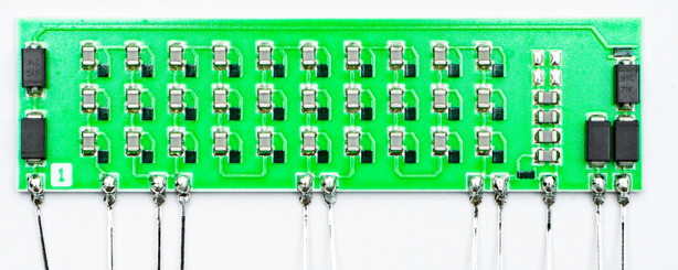
A thick film ceramic board is manufactured using a highly precise, additive screen-printing process. Rather than etching away solid metal, specialized pastes containing conductive metals, resistive elements, or insulating dielectrics are printed onto a bare ceramic substrate through a patterned woven mesh screen.
The conductive pastes typically consist of finely milled metal particles suspended in a glass frit and an organic binder. We generally use silver, palladium-silver, or gold pastes. Once printed, the substrate is dried and then fired in a conveyor furnace at high temperatures, usually around 850 degrees Celsius. During this firing phase, the organic binders burn off while the glass frit melts. This permanently fuses the metallic particles to the ceramic base.
Key Characteristics of Thick Film Technology:
Integrated Passives: The defining feature of this process is the ability to screen-print resistive pastes directly onto the substrate. Technicians actively laser-trim these printed resistors on the production line to achieve exact ohmic values. This completely eliminates the need for discrete surface-mount resistors.
Multilayer Capabilities: By printing alternating layers of conductive traces and insulating glass dielectrics, thick film ceramic circuit boards easily achieve complex 3D multilayer structures. Designs can scale from 3 layers up to 10 layers or more, supporting trace widths and spacings down to 0.1mm.
Environmental Resilience: The fired glass-and-metal matrix creates a hermetic-like seal. It is highly resistant to moisture ingress, extreme temperatures, and chemical degradation.
Direct Bonded Copper utilizes a fundamentally different, subtractive manufacturing approach. Instead of printing metallic pastes, this method involves physically bonding heavy, solid copper foil directly to both sides of a ceramic substrate.
This is achieved through a high-temperature eutectic melting process. The copper and ceramic are heated in a controlled environment containing a specific oxygen concentration. At approximately 1065 degrees Celsius, a thin layer of copper-oxygen eutectic liquid forms. This liquid wets the ceramic surface and creates an incredibly strong chemical bond upon cooling. The solid copper is then patterned using standard photolithography and wet chemical etching.
Key Characteristics of Direct Bonded Copper:
Massive Copper Thickness: This technology utilizes ultra-thick copper layers, typically ranging from 127µm up to 300µm or more.
Extreme Current Capacity: Thanks to the solid copper mass, these boards carry hundreds of continuous amps without overheating. This makes them the standard for heavy-duty industrial drives.
Structural Limitations: Due to the aggressive nature of the chemical etching process, thick copper cannot support complex multilayer routing. It is strictly a 2D technology and cannot integrate printed passive components.
To make an informed engineering decision, teams must compare these two technologies across specific performance metrics. The theoretical capabilities often clash with practical manufacturing constraints on the factory floor.
| Technical Parameter | Thick Film Ceramic Technology | Direct Bonded Copper |
|---|---|---|
| Metallization Process | Additive screen printing & firing at 850°C | Eutectic oxidation bonding at 1065°C & etching |
| Conductor Material | Silver, Palladium-Silver, Gold pastes | Solid Copper foil |
| Conductor Thickness | 10µm to 25µm per printed layer | 127µm to 300µm+ |
| Current Capacity | Low to Moderate up to 20A | Extremely High 100A to 500A+ |
| Multilayer Capability | Excellent with 3 to 10+ layers easily achievable | Poor and typically limited to 1 or 2 layers |
| Passive Integration | Yes via printed monolithic resistors | No, requires discrete SMT soldering |
When evaluating raw electrical conductivity, heavy copper remains unmatched. The thick metal provides minimal electrical resistance. This prevents catastrophic resistive heating under massive current loads. Conversely, a thick film board utilizes thinner conductive traces around 15µm thick. While silver is highly conductive, this thinness means it cannot carry raw traction-inverter amperage.
However, thick film excels in high-voltage isolation. By printing specialized dielectric glass layers, engineers design robust mixed-signal boards. We can establish precise creepage and clearance barriers between high-voltage power sections and sensitive logic controls.
Modern power modules are rarely just dumb power switches. They increasingly incorporate intelligent gate drivers and diagnostic feedback loops. Routing complex control signals alongside power traces on a single copper layer often leads to impossible layout scenarios. It forces engineers to design excessively large boards. Thick film solves this by allowing us to stack circuitry vertically. Power traces run on the bottom layer, while intricate sensor routing is stacked above, safely separated by reliable glass dielectrics.
In high-vibration environments, standard solder joints are the most frequent points of failure. Every discrete surface-mount resistor added to a copper board introduces two potential failure points. Thick film technology circumvents this by printing resistors directly onto the ceramic. These integrated components become a monolithic part of the board. They exhibit excellent stability over extreme temperature variations and significantly reduce parasitic inductance.
Selecting the correct substrate requires a holistic evaluation of thermal dissipation, spatial constraints, and production economics. Here is an objective, practical breakdown of the exact engineering scenarios where printed ceramic technology provides a distinct advantage.
If your layout requires placing a microcontroller right next to a 600V switch to kill gate loop inductance, heavy copper will fail you. Because it relies on etching thick metal, achieving fine line resolution is chemically difficult. The etching process leaves a trapezoidal trace cross-section, which compromises high-density routing.
In contrast, precision screen printing allows conductive pastes to form fine trace widths down to 0.1mm. If your module requires complex gate driver circuitry alongside moderate power switches, thick film seamlessly merges low-power logic with the power stage on a single, highly reliable base.
Miniaturization remains a persistent demand in aerospace and portable medical electronics. When your Z-axis height and X-Y footprint are strictly limited, you cannot afford the real estate required for discrete components. By deploying a thick film integrated circuit substrate, engineers embed resistors directly into the unused spaces between traces. You can stack routing vertically. This 3D integration drastically shrinks the overall size of the module while maintaining excellent thermal contact with the heat sink.
Procurement specialists must factor in tooling costs. The copper bonding manufacturing process is highly capital-intensive. It requires expensive oxidation furnaces and complex photolithography masks. Therefore, it is economically viable primarily for standardized, high-volume mass production.
Printed ceramic processing is inherently more agile. Modifying a layout only requires fabricating new stainless-steel mesh screens. This is a fast and inexpensive process. For specialized industrial equipment, prototyping phases, or custom defense applications, this method offers a significantly lower barrier to entry and a much faster time-to-market.
In automotive engine control units or down-hole drilling equipment, electronics face severe mechanical vibration. Heavy copper boards suffer from a large expansion mismatch between the thick metal layer and the alumina ceramic. This can cause copper delamination over thousands of aggressive thermal cycles.
Printed metallization layers are much thinner and form a robust chemical bond with the ceramic during firing. This results in far lower interfacial stress. For intelligent power modules integrating temperature or pressure sensors in harsh environments, the monolithic nature of printed ceramics provides superior long-term mechanical reliability.
To maintain objective engineering rigor, we must acknowledge where heavy copper remains the undisputed champion. If your design is a pure, ultra-high-power traction inverter switching hundreds of amperes, you must use Direct Bonded Copper or Active Metal Brazing. In these raw power scenarios, there is no substitute for the current-carrying capacity and lateral thermal spreading mass of 300µm solid copper. Printed silver traces would quickly vaporize under such extreme continuous loads.
The unique blend of thermal management, multilayer routing, and integrated passives makes printed ceramic substrates highly sought after across several critical industries:
Automotive Electronics: Utilized extensively in Engine Control Units, transmission modules, and high-power LED headlight drivers where ambient heat and vibration are constant.
Industrial Power Supplies: Ideal for custom DC-DC converters and solid-state relays requiring precise gate-drive resistors and high-voltage isolation barriers.
Aerospace and Defense: Deployed in miniaturized power distribution modules and radar power supplies where failure is not an option and spatial footprint is at an absolute premium.
Telecommunications: Employed in high-frequency RF power amplifiers where exact geometric control of traces ensures minimal signal loss.
Identifying the correct technology is only the first half of the engineering challenge. Executing the design requires partnering with a capable manufacturer. The fabrication of technical ceramics is a highly specialized field demanding strict process controls.
When evaluating a manufacturing partner, engineers should scrutinize the supplier alignment capabilities and firing kilns. A reliable vendor must demonstrate the ability to achieve tight line width tolerances of 0.1mm. This ensures that complex multilayer routing aligns perfectly without shorting. Precision laser trimming capabilities are equally essential if your design relies on integrated resistors to maintain strict voltage sensing parameters.
Slight deviations in furnace atmospheric controls can alter paste resistance values or weaken adhesion. To ensure your concept translates flawlessly to reality, sourcing custom thick film ceramic substrates from an experienced vendor is critical. Manufacturers with deep expertise can help optimize your layout to minimize parasitic inductance and maximize thermal flow.
Engineers must carefully balance thermal requirements with design complexity. While heavy copper handles raw power and extreme current with unmatched efficiency, thick film technology offers unparalleled routing flexibility. By integrating passive components directly into the substrate and supporting dense multilayer architectures, it significantly reduces overall module size and assembly costs.
Carefully evaluate your specific current limits, spatial constraints, and production volumes. For mixed-signal designs, high-vibration environments, or rapid custom prototyping, a tailored ceramic circuit board acts as the precision tool that ensures both performance and economic viability. If your project demands high-density routing and integrated passives, explore the specific ceramic material properties and manufacturing tolerances available at XRmkpcb to match your exact module requirements.
Yes. Thick film ceramics offer excellent dielectric strength. By utilizing specialized multilayer dielectric glass pastes and maintaining proper trace spacing for creepage and clearance, they are highly effective and safe for high-voltage power module applications.
The absolute thermal conductivity is primarily dictated by the base ceramic material. For example, Aluminum Nitride is superior to Alumina in both processes. However, Direct Bonded Copper has an edge in lateral heat spreading due to its thick metal layer. While printed ceramics lack this heavy copper mass, they still provide vastly superior thermal performance compared to standard FR4 boards.
Thin film utilizes vacuum deposition sputtering to create ultra-precise, nanometer-scale lines. This makes it ideal for high-frequency microwave and RF applications. Thick film uses screen printing and high-temperature firing to create micrometer-scale layers, making it more rugged, cost-effective, and suitable for moderate power modules.
Yes, they are highly suitable for low-to-medium power Silicon Carbide and Gallium Nitride modules that require complex, high-speed gate driver integration on the exact same substrate. However, for extreme high-current traction inverters, Active Metal Brazing or Direct Bonded Copper is generally preferred to manage the massive continuous current density.
Thick film ceramic boards can reliably operate at temperatures up to 150°C to 200°C, depending on the specific glass frit and solders utilized in assembly. The fired ceramic and metal matrix is inherently stable, making it exceptionally durable in high-temperature environments.
Absolutely. The tooling and setup costs for screen printing are significantly lower than the expensive photolithography masks and chemical etching required for Direct Bonded Copper. This makes thick film highly cost-effective for prototyping, custom designs, and low-to-medium production runs.


