

Views: 0 Author: Site Editor Publish Time: 2026-09-16 Origin: Site


The demand for efficient heat dissipation in modern electronics is accelerating at an unprecedented rate. Modern devices generate intense, localized heat. Next-generation applications pack immense power into microscopic footprints. Traditional materials simply melt under this pressure. Recent market analyses reveal a dramatic shift in thermal design paradigms. The rapid deployment of 800G optical transceivers in AI data centers and advanced LiDAR systems for autonomous vehicles is driving this structural change. Industry experts note that as chip power densities push past historical limits, thermal management is no longer an afterthought. It has become the primary bottleneck for system reliability.
At the heart of these active cooling systems is the Thermoelectric Cooler, commonly known as a Peltier module. While Peltier devices excel at precise temperature control, the heat they pump to their hot side must be evacuated instantly. If not, thermal runaway occurs. Standard printed circuit board materials consistently buckle under these extreme thermal loads. To resolve this critical bottleneck, engineers are increasingly turning to advanced ceramic thermal management solutions.
However, selecting a bare ceramic base is only half the equation. The core engineering debate today revolves around the two leading metallization technologies used to create these boards: Direct Bonded Copper and Direct Plated Copper. This comprehensive guide objectively analyzes both processes. It provides decision-makers with the technical clarity needed to optimize thermal performance, ensure structural reliability, and maintain cost-efficiency.
TEC Modules Demand Superior Materials: Active cooling requires substrates that deliver exceptionally high thermal conductivity alongside perfect electrical insulation. Traditional FR-4 composites are structurally and thermally inadequate.
DBC Excels in High Power: Featuring thick copper layers and massive current-carrying capacity, DBC remains the industry standard for large-scale industrial cooling applications.
DPC Dominates Micro-Cooling: By leveraging thin-film technology, DPC achieves ultra-fine line resolution and near-perfect surface flatness. This makes it mandatory for miniaturized optical and medical devices.
Context is Everything: The choice between DBC and DPC hinges on a careful engineering balance of power density, spatial constraints, extreme thermal cycling requirements, and manufacturing budgets.
To fully grasp why substrate selection is so unforgiving, one must look at the operational physics of a thermoelectric cooling board. These devices operate on the Peltier effect. When direct current is driven through an alternating array of N-type and P-type semiconductor pellets, heat is actively absorbed on one junction and rejected at the opposite junction.
For this thermodynamic transfer to function without stalling, the substrate holding these delicate pellets must perform two entirely contradictory physical roles. Specifically, it must act as an absolute electrical insulator to prevent catastrophic short circuits between the tightly packed semiconductors. Simultaneously, it must serve as a highly efficient thermal highway. Heat acts like water. If the drain is clogged, it backs up. Any thermal resistance here acts as a dam, causing heat to back up into the module and neutralizing the cooling effect entirely.
Looking closely at standard printed circuit boards, they are primarily fabricated from FR-4. This is a woven fiberglass and epoxy composite. The thermal conductivity of FR-4 hovers around a dismal 0.25 to 0.3 W/m·K. Consequently, when subjected to the aggressive heat fluxes of a Peltier device, FR-4 behaves as a thermal insulator. Even standard Metal Core PCBs, which utilize a dielectric layer between a metal core and copper traces, struggle to push past 3 to 7 W/m·K.
When applied to active cooling environments, these thermal bottlenecks cause rapid heat accumulation. Poor dissipation leads to severe thermo-mechanical stress. The board warps, the dielectric layer degrades, and ultimately, the semiconductor pellets fracture. Upgrading to a specialized ceramic base eliminates the organic dielectric layer entirely. This provides the direct, high-efficiency thermal path that modern electronics demand.
Direct Bonded Copper relies on a rugged, high-temperature manufacturing technique that has served the power electronics industry for decades. The process involves placing bare copper foil in direct contact with a ceramic core, usually Alumina or Aluminum Nitride. The assembly is then introduced into a precisely calibrated atmospheric furnace containing a specific concentration of oxygen.
As temperatures approach 1065°C, a copper-oxygen eutectic melt forms. This liquid chemically reacts with the ceramic surface, wetting it perfectly. Upon cooling, it creates an incredibly robust, direct bond without relying on any intermediate organic adhesives that might impede heat flow.
The most defining advantage of a DBC ceramic PCB is its capacity to support exceptionally thick copper layers. Ranging from 100µm up to 300µm, this massive copper cross-section provides outstanding current-carrying capacity. For instance, elongated DBC ceramic substrates designed for large TECs can easily support massive amperage without breaking a sweat. For large, high-wattage TEC modules, this thickness prevents the circuit traces from overheating.
Furthermore, because the copper is bonded directly to the ceramic, interfacial thermal resistance is virtually zero. The thick copper acts as an aggressive lateral heat spreader. It diffuses concentrated thermal energy across a wider area of the board before passing it down into the heatsink. From a manufacturing standpoint, DBC is highly mature. This makes it remarkably cost-effective for large-scale, industrial-grade cooling systems.
Despite its ruggedness, DBC carries inherent physical limitations. The extreme temperatures required for eutectic bonding can occasionally trap microscopic oxygen bubbles. This results in subtle dimples or micro-voids at the copper-ceramic interface. While generally harmless in massive industrial modules, these voids can create localized hot spots in high-precision devices.
More importantly, DBC struggles with miniaturization. Because the copper layers are so thick, etching circuit patterns requires aggressive wet chemical processes. This etchant removes copper from the sides of the traces as well as the top, leading to severe undercutting. As a result, DBC cannot reliably achieve the fine-pitch, high-density circuit routing required by today's smart, miniaturized devices.
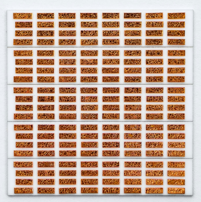
In stark contrast to the brute-force heat of DBC, Direct Plated Copper borrows precise thin-film techniques directly from the microchip industry. The process begins inside a vacuum chamber. A microscopic titanium or chromium adhesion layer is deposited onto the bare ceramic using Physical Vapor Deposition, specifically magnetron sputtering. A thin seed layer of copper immediately follows.
Once this foundation is laid, engineers utilize high-resolution photolithography to apply a photoresist mask. This defines the exact circuit pattern with microscopic accuracy. Finally, electroplating builds up the copper thickness only where it is explicitly required. The photoresist is then stripped away, and the background seed layer is gently etched off.
Because the circuit layout is defined by light rather than aggressive chemical etching, a DPC ceramic substrate completely sidesteps the undercutting issues of DBC. It can reliably achieve ultra-fine line widths and tight spacing down to 50µm or less. This unmatched precision makes DPC the definitive choice for micro-coolers used to stabilize laser diodes, LiDAR sensors, and implantable medical diagnostics.
In addition, the sputtering and plating processes yield an exceptionally flat copper surface with incredibly low roughness values. In TEC assembly, surface planarity is paramount. Any microscopic unevenness creates tiny air gaps between the semiconductor dies and the board. Since air is a notorious thermal insulator, these gaps cripple heat transfer. DPC ensures maximum interfacial contact, optimizing thermal flow. Moreover, the low-temperature vacuum process prevents the introduction of residual thermal stress within the ceramic core, enhancing overall mechanical stability.
The primary hurdle for DPC technology is its cost profile. The reliance on expensive vacuum sputtering equipment and cleanroom photolithography makes manufacturing inherently more expensive than DBC. While DPC copper can be plated to moderate thicknesses, typically 10µm to 100µm, attempting to electroplate the massive 300µm layers found in DBC becomes highly time-consuming and economically unviable. Therefore, DPC is rarely specified for massive, high-current industrial chillers.
Both technologies leverage the excellent baseline thermal conductivity of their respective ceramic cores. Yet, their heat dissipation mechanics differ significantly based on their surface structures. DBC excels in macro-scale thermal management. Its massive copper volume acts as a highly effective heat spreader, rapidly diffusing intense, localized heat loads from large Peltier elements. Conversely, DPC offers superior vertical thermal transfer for micro-scale components. Its ultra-flat surface eliminates insulating air voids, allowing for direct die attachment with absolute minimal thermal resistance.
In real-world applications, TEC modules endure brutal thermal cycling. Consider an aerospace component or an environmental test chamber where a module must rapidly drop to -30°C and then surge back to ambient temperatures. This rapid fluctuation introduces severe thermo-mechanical stress due to the mismatch in the coefficient of thermal expansion between the expanding copper and the rigid ceramic.
While DBC boasts high initial bond strength, its thick copper exerts massive shear forces on the ceramic during these extreme temperature swings. If not meticulously designed, this stress can trigger microscopic cracking or delamination over thousands of cycles. DPC is formed at much lower temperatures with thinner copper. It retains far less internal residual stress. Consequently, it frequently demonstrates superior reliability and longevity under aggressive, rapid thermal cycling conditions.
Modern thermal management often requires integrating thermistors, control logic, or sensor arrays directly onto the same substrate as the cooling elements. DBC is physically incapable of meeting these tight design rules due to its wide trace requirements. For highly integrated, smart cooling assemblies, the photolithographic precision of DPC is not just an advantage. It is a strict engineering necessity.
| Feature / Engineering Metric | DBC Direct Bonded Copper | DPC Direct Plated Copper |
|---|---|---|
| Metallization Process | High-temp Eutectic Melting 1065°C | Vacuum Sputtering PVD + Electroplating |
| Typical Copper Thickness | 100µm – 300µm+ Thick | 10µm – 100µm Thin to Moderate |
| Line Resolution Min Trace/Space | > 150µm Wide traces due to etching | < 50µm Ultra-fine pitch |
| Surface Flatness | Moderate Prone to micro-dimples | Excellent Near-perfect planarity |
| Thermal Cycling Reliability | Good High shear stress under extremes | Excellent Low internal residual stress |
| Ideal Application Match | Large industrial coolers, high-power modules | Micro-coolers, optical transceivers, medical devices |
Specifying the right metallization process dictates how current flows and how components are attached. However, the foundation itself dictates the ultimate thermal bottleneck. The ceramic core is solely responsible for moving heat vertically through the board to the heatsink. If the ceramic's thermal conductivity is too low for the application's heat flux, neither DBC nor DPC will save the system from overheating.
Alumina, typically 96% purity, serves as the dependable workhorse for commercial TEC modules. Offering a thermal conductivity of approximately 24 to 30 W/m·K, it is nearly 100 times more efficient than standard FR-4. Alumina is highly cost-effective and mechanically robust. It is perfectly suited for consumer refrigeration, standard electronics cooling, and budget-conscious industrial applications.
When engineering for extreme-performance environments, Aluminum Nitride is the undisputed material of choice. AlN boasts an exceptional thermal conductivity ranging from 170 to 230 W/m·K. This approaches the thermal transfer rates of metallic aluminum, but with total electrical isolation. Furthermore, AlN possesses a thermal expansion coefficient that closely mirrors silicon semiconductor chips. This critical matching drastically reduces mechanical shear stress during thermal cycling. This makes AlN the premier choice for aerospace, high-power lasers, and mission-critical applications where failure is not an option.
Engineers should specify a DBC substrate when the project involves:
High power output and substantial electrical current requirements.
A larger physical footprint where trace density and spacing are not limiting factors.
Standard industrial cooling systems and automotive climate control.
Budget-conscious projects that require thick copper for aggressive lateral heat spreading.
Conversely, engineers should opt for a DPC substrate when the application demands:
Micro-coolers designed for telecommunications, LiDAR, or optical transceivers.
High-density packaging requiring ultra-fine circuit traces and complex routing.
Strict surface flatness requirements to ensure flawless semiconductor die attachment.
Aggressive thermal cycling profiles where minimizing residual mechanical stress is critical to product longevity.
Achieving optimal thermal dynamics requires flawless manufacturing execution. Minor variations in the eutectic bonding of DBC or the vacuum sputtering environment of DPC can introduce hidden thermal resistances. These invisible defects degrade module performance. Therefore, it is absolutely vital to collaborate with an experienced manufacturer who rigorously understands the strict tolerances and material sciences behind advanced TEC ceramic substrate fabrication.
Choosing the right substrate for a Peltier device is a critical engineering decision that directly impacts system reliability. Neither DBC nor DPC is universally superior. The correct choice depends entirely on a careful analysis of your specific thermal loads, spatial constraints, and electrical requirements. By optimizing your thermoelectric module with the appropriate ceramic core and metallization process, you effectively eliminate thermal bottlenecks, extend product lifespan, and maximize cooling efficiency. Stop guessing with your thermal management. Consult with experts early in your design phase and visit XR MK PCB to find the exact ceramic substrate solution that ensures your next project operates flawlessly under pressure.
Yes, Active Metal Brazing is another valid metallization option. It is primarily utilized in conjunction with Silicon Nitride ceramic cores. AMB offers the highest possible mechanical reliability and bonding strength, making it ideal for extreme automotive or aerospace environments. However, the manufacturing cost of AMB is significantly higher than both DBC and DPC. For the vast majority of standard and even high-performance TEC applications, AMB is considered over-engineered and unnecessary. This makes DBC or DPC the much more practical and economical choices.
Absolutely. In the realm of thermal dynamics, any microscopic unevenness on the substrate creates tiny air gaps between the TEC semiconductor components and the board surface. Because air has a terrible thermal conductivity, it acts as a severe thermal insulator. This degrades the overall cooling efficiency of the system. DPC technology provides superior surface planarity, ensuring maximum physical contact and optimal heat transfer. This is exactly why it is heavily favored for precision micro-coolers.
The DBC process is specifically engineered to handle heavy copper. It can comfortably support copper thicknesses ranging from 100µm to 300µm. In specialized heavy-industrial applications, it can be pushed even thicker. This massive copper volume is highly suitable for safely carrying the high electrical currents required by large, high-wattage Peltier modules without overheating the circuit traces.
Yes. The DPC manufacturing process relies on physical vapor deposition and electroplating. Both of these occur at significantly lower temperatures compared to the intense eutectic melting required for DBC. This results in a finished substrate with much lower internal residual stress. When DPC is paired with an Aluminum Nitride core, the resulting board performs exceptionally well under rapid and extreme thermal cycling without the risk of trace delamination or ceramic cracking.
Copper thickness directly influences both electrical resistance and lateral heat spreading. Thicker copper, typically found in DBC boards, reduces electrical resistance, allowing high-power modules to draw more current without generating excess Joule heating in the traces. Additionally, thick copper acts as a lateral heat spreader, diffusing concentrated heat spots across a wider area before it enters the ceramic core. However, for micro-coolers, overly thick copper is unnecessary and prevents the fine-pitch routing needed for miniaturization.
Not always. While Aluminum Nitride provides vastly superior thermal conductivity, it is also significantly more expensive than Alumina. For low-power consumer devices or standard refrigeration units where the heat flux is manageable, Alumina is more than sufficient and keeps manufacturing costs down. Aluminum Nitride becomes strictly necessary only when dealing with high power densities, such as in laser diodes or optical transceivers, where Alumina would cause heat to back up into the system.


