

Views: 0 Author: Site Editor Publish Time: 2026-08-27 Origin: Site


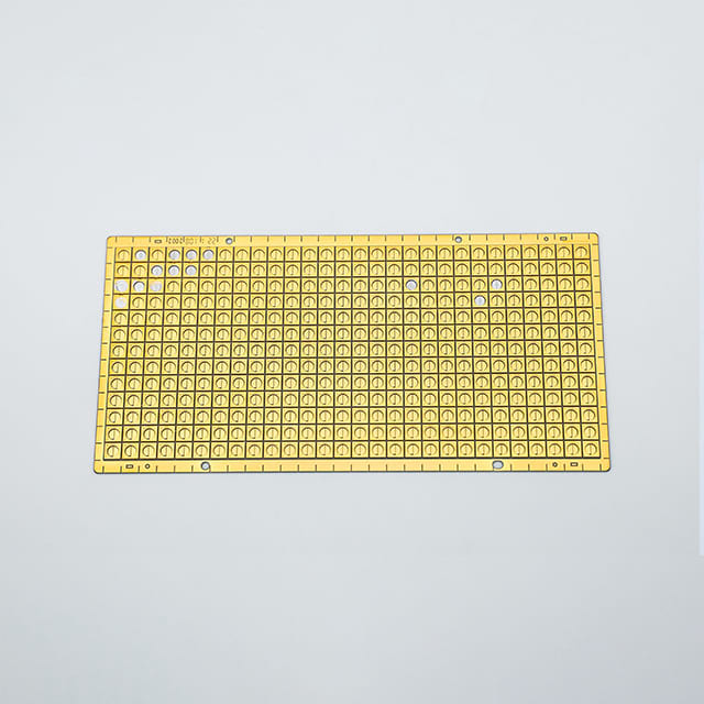
Pad geometry at the bare-board level dictates the success or failure of advanced microelectronics assembly. A direct correlation exists between poorly specified pad dimensions and catastrophic manufacturing failures. Components suffer from cracking, tombstoning, and severe misalignment when pad layouts ignore the physical realities of the reflow process. Engineering teams constantly face a strict tension. You must increase package density to route additional signals, yet you remain bound by the physical limitations of maintaining tight geometric tolerances during assembly. Ignoring these limits results in massive yield loss and expensive rework cycles.
This guide serves as a technical evaluation framework for engineering and procurement teams. You will learn how to align pad design specifications with the manufacturing realities of a ceramic packaging substrate. We evaluate the exact mechanics required to ensure reliable solder joint formation and long-term mechanical stability. Proper pad optimization prevents bridging, controls solder paste volume, and guarantees predictable component self-alignment.
Pad geometry directly dictates solder paste volume, wetting dynamics, and component self-alignment during reflow, serving as the primary baseline for assembly yield.
High-density routing in advanced ceramic packages requires strict control over pad tolerances to prevent bridging and poorly formed fillets.
Selecting between Solder Mask Defined (SMD) and Non-Solder Mask Defined (NSMD) pads on ceramic substrates fundamentally alters thermal cycling reliability and stress distribution.
Evaluating a substrate manufacturer’s capability to hold precise dimensional tolerances is a critical procurement gate for high-power and sensor applications.
A successful pad geometry must meet strict mechanical and metallurgical criteria. You need an optimal aspect ratio to support the specific component termination. Predictable paste coverage ensures the exact volume of flux and alloy transfers during printing. The pad must provide sufficient exposed area for robust intermetallic compound (IMC) formation. If the pad lacks adequate surface area, the IMC layer becomes dangerously thin. This compromises the mechanical bond. Success means achieving a geometry yielding zero defects during automated optical inspection while surviving accelerated thermal cycling tests.
Engineers often rely on IPC-7351 standards as a baseline, but ceramic materials require specific deviations. Alumina and aluminum nitride dissipate heat differently than standard FR4. This thermal reality means your pad geometry must account for faster heat extraction during the reflow profile. If the pad is too small, the joint starves. If the pad is too large, the component floats. You must calculate the exact wettable surface area required to anchor the component while allowing the solder to form a structurally sound fillet.
Pad shape and size strictly control the volume of solder forming the final fillet. Rectangular, circular, and oblong pads each interact differently with molten solder. When you specify an incorrect geometry, the reflow process produces a poorly formed fillet. A fillet lacking the correct concave profile creates a weak joint. This weak joint becomes highly susceptible to thermal-mechanical cracking. Ceramic materials possess unique thermal conductivity profiles. This alters how heat transfers into the joint during reflow.
If the pad is too short, the heel fillet cannot form properly. The heel fillet provides the primary mechanical strength for gull-wing leads. If the pad is too narrow, the side fillets vanish. Both scenarios drastically reduce the shear strength of the assembled component. You must design the pad extension beyond the component lead to allow the molten solder to climb the termination. A proper heel and toe fillet requires a pad extension of at least 0.2mm to 0.5mm depending on the component pitch and lead thickness.
Surface tension during reflow dictates component alignment. Molten solder exerts a powerful pulling force. Symmetrical and accurately dimensioned pads facilitate perfect self-centering. As the alloy turns liquid, surface tension equalizes across the component terminations. This pulls the part into exact alignment. Conversely, asymmetrical geometries cause immediate skewing. If one pad is larger than its pair, it pulls harder. The component rotates or shifts off-axis.
You must balance the wettable surface area perfectly across all mounting points to harness surface tension effectively. This becomes exceptionally difficult with passive components like 0201 or 01005 resistors. A deviation of just a few microns in pad width creates enough force imbalance to twist the component off its axis. Layout designers must ensure that traces entering the pads do not act as heat sinks. A wide trace entering one pad and a narrow trace entering the other will cause the solder to melt at different times, destroying the self-alignment process.
The Direct Plated Copper (DPC) process revolutionizes pad precision. DPC utilizes high-resolution thin-film technology combined with vacuum sputtering and photolithography. This allows you to achieve exceptionally tight pad geometries. Traditional thick-film screen printing struggles with edge definition. DPC delivers vertical sidewalls and sharp pad edges. A DPC ceramic package substrate supports superior vertical interconnects and ultra-fine pitch routing.
You can design pads with tolerances previously restricted to silicon wafers. This precision eliminates the standard manufacturing deviations causing solder bridging in high-density layouts. When working with DPC, you can push pad pitches down to 50 microns or less. The sputtered titanium or chromium adhesion layer ensures the copper pad remains firmly anchored to the ceramic, even under extreme shear stress. This allows for smaller pad sizes without sacrificing mechanical reliability.
Manufacturing Tolerance Comparison
| Technology | Minimum Pad Pitch | Edge Definition | Surface Planarity | Best Application |
|---|---|---|---|---|
| Thick Film Printing | 150 - 200 microns | Sloped / Irregular | Moderate | Standard automotive, industrial controls |
| Direct Plated Copper (DPC) | 30 - 50 microns | Vertical / Sharp | Excellent | High-density LED, fine-pitch flip-chip |
High-Temperature Co-fired Ceramic (HTCC) and Low-Temperature Co-fired Ceramic (LTCC) technologies rely on multi-layer lamination. Electrical circuit patterns are applied to individual green ceramic layers. These layers are then stacked and fired to achieve space-saving, three-dimensional routing. Pad geometry and via alignment must be strictly controlled across these laminated layers. During the co-firing process, ceramic materials shrink.
If you do not calculate shrinkage tolerances accurately, the surface pads will misalign with the internal vertical interconnects. This misalignment degrades signal integrity and creates localized high-resistance points. LTCC typically shrinks between 10% and 15% in the X and Y axes during firing. You must scale your pad designs in the CAD software to account for this exact shrinkage rate. Failure to do so results in pads that are too small and improperly spaced, making automated assembly impossible.
Pads serve a dual role in high-power applications. They provide electrical routing and facilitate critical thermal dissipation. You face strict trade-offs when designing a high power packaging substrate. You must maximize the thermal pad area to pull heat away from active die. However, you must simultaneously maintain sufficient isolation gaps to prevent electrical shorting under high voltage.
Large thermal pads often cause solder voiding if outgassing channels are ignored. You must segment large thermal pads into grid patterns. This allows flux volatiles to escape during reflow, ensuring a void-free thermal interface. IPC-A-610 Class 3 standards require voiding to remain below 20% of the total thermal pad area. By breaking a massive 10mm x 10mm pad into a matrix of smaller 2mm x 2mm pads connected by a solder mask web, you provide escape routes for the gas. This simple geometric modification drastically reduces voiding and improves thermal transfer.
Hermetic sensor packaging demands absolute geometric precision. Pad flatness and edge definition directly impact the reliability of wire bonding and flip-chip attach. A sensor packaging ceramic substrate operates in sensitive environmental conditions. Any surface irregularity on the wire bond pad causes non-stick on pad (NSOP) defects.
Gold or aluminum wire bonds require a pristine, perfectly flat bonding area. For flip-chip sensors, uneven pad heights cause stress concentrations on specific solder bumps. This uneven stress fractures the delicate sensor die during operational thermal cycling. Wire bond pads must maintain a surface roughness (Ra) of less than 0.1 microns. The geometry must also provide a target area at least 2.5 times the diameter of the wire being bonded to ensure the capillary tool has sufficient landing space.
Oversized pads lead directly to solder starvation at the joint. The molten alloy spreads too far across the excessive pad area. This leaves insufficient volume to climb the component termination, causing poor wetting and weak mechanical bonds. Conversely, undersized pitch or excessive pad width causes bridging. When pads sit too close together, the solder paste merges during printing or reflow. This creates hard electrical shorts.
You must calculate the exact pad width to accommodate the component lead while maintaining a safe isolation gap based on the specific solder alloy's wetting characteristics. For fine-pitch QFN packages, the pad width should typically be 60% to 80% of the component lead width. This prevents the solder from bulging outward and touching the adjacent pad. You must also account for the solder mask registration tolerance. If the mask shifts, it can expose adjacent copper, creating an unintended bridge path.
Tombstoning occurs when one end of a passive component lifts off the pad during reflow. Uneven pad geometries cause a severe thermal imbalance. If one pad connects to a massive copper plane while the other connects to a thin trace, they heat at different rates. The solder on the hotter pad melts first. Its surface tension pulls the component upright. Skewing happens in active die when asymmetrical pads cause unequal pulling forces.
You must ensure thermal relief connections and perfectly matched pad dimensions to prevent these dynamic reflow failures. When routing a trace into a pad, use a neck-down technique. Reduce the trace width just before it enters the pad to minimize heat sinking. Ensure both pads of a two-terminal component have identical copper weight and trace connections. This guarantees they reach the liquidus temperature simultaneously.
Via-in-pad designs save valuable surface space but introduce severe reliability risks. Data from IPC HDPUG and SMTA studies highlight these exact challenges. Uncapped vias act as capillary tubes. They wick molten solder away from the joint and down into the via barrel. This leaves the component starved of solder, causing open circuits. Voiding also increases as trapped air escapes from the via during reflow.
You must implement strict via filling and capping protocols. Plating over filled vias (POFV) is an absolute necessity to maintain joint integrity on high-density layouts. The process requires specific steps to ensure reliability.
Drill the via mechanically or with a laser depending on the required diameter.
Plate the via barrel with copper to establish the electrical connection.
Fill the via completely with a specialized conductive or non-conductive epoxy resin.
Planarize the surface to remove any excess epoxy and create a perfectly flat substrate.
Plate a final layer of copper over the filled via to create a continuous, solid solder pad.
Skipping any of these steps results in dimpled pads. A dimple larger than 15 microns will trap air during solder paste printing, leading directly to massive voids in the final BGA or QFN joint.
Choosing between Solder Mask Defined (SMD) and Non-Solder Mask Defined (NSMD) pads fundamentally alters stress distribution. SMD pads use the solder mask to define the wettable area. This provides better pad adhesion to the substrate but creates high stress concentration at the mask edge. NSMD pads leave a gap between the pad and the mask. The solder grips the top and sides of the pad. This yields better solder joint reliability but requires tighter clearance tolerances.
Pad Configuration Comparison
| Configuration Type | Adhesion Strength | Solder Joint Reliability | Clearance Requirements | Primary Application |
|---|---|---|---|---|
| Solder Mask Defined (SMD) | High (Mask overlaps pad) | Lower (Stress at mask edge) | Standard | High thermal mass components |
| Non-Solder Mask Defined (NSMD) | Standard | High (Solder wraps pad edges) | Strict (Requires tight registration) | BGA and fine-pitch flip-chip |
You must choose the configuration based on the specific ceramic material. Alumina and Aluminum Nitride possess different adhesion characteristics. NSMD is generally preferred for fine-pitch assembly to maximize thermal cycling fatigue resistance. When using NSMD, the copper pad diameter should be 20% smaller than the BGA sphere diameter to allow the solder to wrap around the pad edges effectively. This wrapping action increases the shear strength of the joint by up to 30% compared to a flat SMD joint.
Large flip-chip die assembly presents unique geometric challenges. Routing all additional I/O signals in higher-density packages makes maintaining tight tolerances exceedingly difficult. Industry studies document the strain placed on outer solder bumps. You must specify pad designs accommodating the coefficient of thermal expansion (CTE) mismatch. Silicon die expand at roughly 2.6 ppm/C. Alumina substrates expand at roughly 7.0 ppm/C.
This mismatch shears the solder bumps during thermal cycling. You must optimize pad diameters to maximize the standoff height of the solder bump, allowing it to absorb the thermomechanical strain. A smaller pad diameter on the substrate forces the solder bump to stand taller. A taller bump acts like a flexible pillar, absorbing the lateral shear forces generated by the CTE mismatch. You must also specify a high-quality underfill material to encapsulate the bumps and distribute the stress evenly across the entire die footprint.
Pad geometry must be co-designed with stencil aperture dimensions. You cannot design pads in isolation. The area ratio of the stencil aperture dictates transfer efficiency during solder paste printing. If the pad is too small relative to the stencil thickness, the paste sticks inside the aperture. This causes insufficient paste volume on the pad. You must calculate the exact aspect ratio to ensure consistent paste release.
The Area Ratio is calculated by dividing the area of the aperture opening by the area of the aperture walls. Industry standards dictate that the Area Ratio must be greater than 0.66 for reliable paste release. If your pad geometry forces an aperture design with an Area Ratio below 0.66, you must either increase the pad size or specify a thinner stencil foil. Proper alignment between pad geometry and stencil design prevents bridging, minimizes voiding, and guarantees the correct solder volume for robust fillet formation.
Theoretical pad designs often face harsh manufacturing deviations. You must account for the etch factor during copper patterning. Traces and pads form a trapezoidal shape rather than a perfect rectangle due to chemical etching dynamics. The top of the pad will always be slightly narrower than the base. Plating thickness variations alter the final surface topography. Substrate shrinkage during ceramic firing introduces dimensional shifts.
If you design pads at the absolute minimum tolerance limit, normal manufacturing variations will push your boards into failure. You must build acceptable tolerance bands into your initial layout. Work directly with your fabrication facility to understand their specific etch-back allowances. If you require a final pad width of 100 microns, you may need to draw the pad at 115 microns in your CAD software to compensate for the etching process.
Never move directly to high-volume production without rigorous pilot runs. Implement strict Design for Manufacturability (DFM) checks before finalizing Gerber files. Utilize automated optical inspection (AOI) on bare substrates to verify pad dimensions and edge definition. Conduct cross-sectional analysis of initial solder joints from the pilot run.
Cross-sectioning reveals the true IMC layer thickness and exposes hidden voiding within the fillet. These mitigation strategies catch geometric flaws before they cause massive yield loss on the assembly line. You should also implement Solder Paste Inspection (SPI) during the pilot run. SPI uses 3D scanning to measure the exact volume, height, and area of the printed solder paste on every single pad. This data allows you to fine-tune your stencil apertures and pad geometries before committing to full production.
Vetting your substrate manufacturer is a critical procurement gate. You must evaluate their specific capabilities regarding pad geometry. Do not rely on marketing brochures; demand hard engineering data.
Verify their minimum reliable pad size and minimum pitch capabilities through physical sample inspection.
Audit their dimensional tolerance controls for etching and plating processes, requesting their standard deviation data.
Request historical yield data specifically for complex, high-density ceramic packages similar to your design.
Assess their ability to perform precise via filling and planarization for via-in-pad designs, checking for dimple depth specifications.
Confirm their experience with the specific ceramic technology required, whether it is DPC, HTCC, or LTCC.
Review their automated optical inspection (AOI) equipment capabilities to ensure they can actually measure the fine-pitch geometries you require.
Take the following actions immediately to secure your assembly yield:
Initiate a formal design review of your current pad layouts with your chosen assembly partner and substrate fabricator.
Audit your bare-board specifications against the manufacturer's actual etching, plating, and shrinkage tolerances.
Implement strict via-capping and planarization rules for all via-in-pad locations to prevent solder wicking and voiding.
Run a pilot build dedicated solely to cross-sectional analysis and 3D solder paste inspection of the joint fillets.
Adjust your CAD libraries to ensure all thermal relief connections are perfectly balanced to prevent tombstoning.
A: Pad geometry determines the volume of solder and the shape of the resulting fillet. Correct dimensions ensure proper wetting and sufficient intermetallic compound formation. Incorrect geometry leads to weak, malformed joints that easily crack under thermal-mechanical stress.
A: Solder Mask Defined (SMD) pads use the mask to define the bonding area, offering better pad adhesion but higher stress concentration. Non-Solder Mask Defined (NSMD) pads leave a gap, allowing solder to grip the pad edges, which significantly improves thermal cycling reliability.
A: Uncapped vias act as capillary tubes during reflow. They wick molten solder away from the component termination and down into the via barrel. This causes solder starvation, open circuits, and severe voiding, compromising both electrical and thermal pathways.
A: Large flip-chip die require ultra-fine pitch routing. Tight pad tolerances are mandatory to prevent solder bridging between adjacent bumps. Precise pad sizing also maximizes bump standoff height, which is critical for absorbing stress caused by CTE mismatch between the silicon and ceramic.
A: DPC technology utilizes thin-film sputtering and photolithography, allowing for extremely fine features. While thick-film limits pitch to larger dimensions, DPC can routinely achieve pad pitches below 50 microns, supporting ultra-high-density microelectronic packaging.
A: Unequal pad sizes create a thermal imbalance. The smaller pad heats faster, melting its solder paste first. The surface tension of the molten solder pulls the component upright before the opposite pad can melt and anchor the other side.
A: Pad flatness is critical for wire bonding and flip-chip attach. Surface irregularities cause non-stick on pad (NSOP) defects during wire bonding. In flip-chip applications, uneven pads create localized stress concentrations that can fracture sensitive sensor die during operation.


