


Views: 0 Author: Site Editor Publish Time: 2026-05-25 Origin: Site


As silicon carbide (SiC) and gallium nitride (GaN) push power densities higher, electronics face unprecedented thermal loads. Meanwhile, 5G/6G applications now demand frequencies above 30 GHz for high-speed data transmission. In these aggressive environments, traditional organic and metal-core boards quickly become the primary bottleneck for system reliability.
Engineers increasingly battle severe thermal stress in modern electronics. Industry research shows this heat causes roughly 55% of early power module degradation. Legacy materials simply cannot support the extreme dielectric and thermal requirements modern chips generate.
A 3D Ceramic Packaging Substrate bridges the gap between bare die limitations and system-level thermal demands. It replaces planar compromises by using integrated, thermally matched vertical routing. You will learn how shifting to advanced ceramics significantly extends device lifecycles and outperforms traditional substrates.
Thermal & Mechanical Symbiosis: 3D ceramic substrates offer a Coefficient of Thermal Expansion (CTE) that closely matches semiconductor materials (4–10 ppm/°C), practically eliminating the shear stress found in organic boards during thermal cycling.
Vertical Integration: Unlike 2D PCBs, a multilayer ceramic substrate allows for 3D electrical routing, embedded passive components, and hermetic cavity structures.
Shift to Active Reliability: Upgrading to advanced ceramics (like AlN or Si3N4) and robust metallization (AMB) can lower operating temperatures by 18°C–24°C, significantly extending device lifecycles in harsh environments like EV traction inverters or aerospace radar.
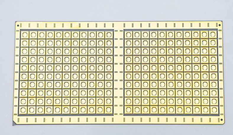
When you hear the term "3D architecture" in advanced packaging, it means much more than a flat mounting surface. We define "3D" through the multi-layered co-firing process. Manufacturers use Low-Temperature Co-fired Ceramics (LTCC) or High-Temperature Co-fired Ceramics (HTCC) to build these structures. They stack multiple thin ceramic layers, integrating blind vias, buried vias, embedded circuitry, and precision cavity structures directly into the matrix. This vertical integration sets it apart from traditional flat boards.
Traditional FR-4 and organic substrates struggle significantly when compared to ceramics. Polymers act as thermal insulators. They typically offer a thermal conductivity of around 0.25 W/m·K. Furthermore, organic boards suffer from glass transition (Tg) degradation at high temperatures. They soften and lose structural integrity. Ceramics easily exceed 20 to 170 W/m·K. They maintain complete structural integrity up to 350°C without softening.
From a mechanical and chemical standpoint, organic materials also introduce contamination risks. Traditional substrates outgas in high-vacuum environments. You often see this problem in Extreme Ultraviolet (EUV) lithography equipment. They also absorb moisture over time. Ceramics remain purely inorganic. They are inherently hermetic and feature zero outgassing, ensuring ultra-clean operation in sensitive environments.
Many engineers wonder how ceramics compare to Metal Core PCBs (MCPCBs). MCPCBs handle heat reasonably well. However, they rely on a metal base covered by thick dielectric layers. These dielectric layers impede optimal thermal transfer. They also severely limit high-frequency electrical performance. A Multilayer ceramic substrate eliminates the need for thick polymer dielectrics. It provides a direct, highly conductive path for both heat and high-frequency signals.
Legacy boards routinely fail under the intense thermal cycling of modern high-power chips. We call this the CTE mismatch trap. When a high-power SiC or GaN chip heats up, the physical materials react differently. Organic boards expand drastically faster than the bare silicon die. This unequal expansion pulls on the connection points. It leads directly to solder joint fatigue, layer delamination, and eventual catastrophic failure.
High-frequency communications introduce another major failure mode: dielectric loss. At high gigahertz ranges, standard PCB resins act like sponges. They absorb signal energy and convert it into useless heat. This ruins signal integrity for 5G and 6G applications. Advanced glass-ceramic substrates solve this physical limitation. They achieve ultra-low dielectric loss (tan δ < 10^-3). They also provide the stable dielectric constants required for pristine signal integrity at high frequencies.
Finally, legacy substrates degrade rapidly in harsh environments. Standard polymer boards break down when exposed to continuous ultraviolet (UV) light, plasma, or extreme cold (-100°C). Chemical bonds in the resin deteriorate. Ceramics remain chemically inert. They stay dimensionally stable regardless of radiation exposure or cryogenic freezing. This makes them the only viable choice for aerospace, deep-sea, and intense industrial applications.
Choosing the correct ceramic matrix requires understanding specific engineering trade-offs. You must balance thermal conductivity, mechanical strength, and material cost. We evaluate the four primary ceramic materials below.
| Ceramic Material | Thermal Conductivity | Key Strength | Ideal Application |
|---|---|---|---|
| Alumina (Al2O3) | ~25 W/m·K | Cost-effective, good baseline strength | Standard industrial power modules |
| Aluminum Nitride (AlN) | 140–170 W/m·K | Exceptional heat dissipation | High-density optoelectronics, lasers |
| Silicon Nitride (Si3N4) | ~90 W/m·K | Superior fracture toughness | 800V+ EV traction inverters |
| Glass-Ceramics (LTCC) | 3–5 W/m·K | Ultra-low dielectric loss, 3D routing | High-frequency 5G/6G RF packages |
Alumina (Al2O3) remains the legacy standard for ceramic boards. It is highly cost-effective. It offers decent thermal conductivity around 25 W/m·K and provides reliable mechanical strength. You will find it works perfectly for standard industrial power modules where budget constraints dictate design choices.
Aluminum Nitride (AlN) stands out as the thermal champion. It delivers exceptional heat dissipation, ranging from 140 to 170 W/m·K. It also provides precise CTE matching for silicon. However, AlN comes with higher raw material and machining costs. It is ideal for high-density optoelectronics, laser diodes, and extreme heat flux scenarios.
Silicon Nitride (Si3N4) operates as the mechanical powerhouse. It has a lower thermal conductivity than AlN, but it boasts superior fracture toughness. It handles bending stress exceptionally well. Si3N4 is the current default choice for 800V+ automotive fast-charging systems. It effortlessly endures the severe physical vibrations found in electric vehicle drivetrains.
Glass-Ceramics (LTCC) serve as the RF specialist. The manufacturing process allows for low-temperature co-firing. They sinter below the melting point of highly conductive metals like silver and copper. This enables highly complex, miniaturized 3D RF packages. They deliver unparalleled high-frequency electrical performance for next-generation telecommunications.
A ceramic substrate is ultimately only as good as its copper-to-ceramic bond. Engineers often overlook metallization, yet it remains a primary reliability bottleneck. How you attach the conductive copper layer to the ceramic base dictates the module's lifespan.
Direct Bond Copper (DBC) is the traditional high-power choice. The DBC process bonds copper directly to alumina or aluminum nitride. It offers excellent electrical and thermal conductivity. However, it can suffer from micro-cracking during extreme thermal cycling. The rigid nature of the bond struggles when subjected to rapid, extreme temperature swings.
Active Metal Brazing (AMB) provides the ultimate reliability upgrade. This process uses active metals, typically titanium, to chemically bond the copper to the ceramic. AMB is especially critical when working with Silicon Nitride (Si3N4). The process costs more, but it drastically improves peel strength. It boosts thermal cycling endurance for mission-critical EV systems and aerospace applications.
Design-for-Manufacturability (DFM) risks pose another hidden challenge. Specifying the wrong metallization thickness can physically warp the ceramic base. You must ensure structural balance. To avoid assembly failures, follow these DFM best practices:
Match Copper Thickness: Ensure the top and bottom copper layers have symmetrical thicknesses to prevent thermal bowing.
Run Co-Simulations: Always perform thermal-mechanical co-simulation before sending designs to prototyping.
Specify Etch Tolerances: Account for the chemical etching limits of thick copper lines to prevent short circuits.
Select the Right Paste: Choose the appropriate brazing paste that matches the specific ceramic CTE profile.
Engineers and purchasing teams must face the pricing reality early in the design phase. A sophisticated ceramic substrate has a noticeably higher upfront Bill of Materials (BOM) cost than standard FR-4 or MCPCBs. You cannot evaluate these materials purely on a per-unit cost basis.
True economic justification emerges when you analyze system-level Return on Investment (ROI). Advanced ceramics drive down associated hardware costs in several key ways:
Cooling Infrastructure Reduction: High thermal conductivity inherently spreads and dissipates heat faster. This reduces your reliance on complex, heavy liquid-cooling systems. You save significant physical space and weight in automotive and aerospace designs.
Lifecycle Extension: Operating high-power modules just 20°C cooler exponentially increases the Mean Time Between Failures (MTBF). This reliability spike slashes warranty claims. It drastically reduces expensive field-replacement costs over the product's lifespan.
Miniaturization Value: Multilayer vertical routing capabilities shrink the physical footprint of the final package. This miniaturization allows for smaller end-devices. It also yields more functional units per production panel, offsetting the initial material expenses.
When you account for smaller cooling requirements, fewer field failures, and highly optimized layouts, the initial investment in ceramic technology pays massive dividends.
Transitioning to a 3D ceramic packaging architecture is not a simple drop-in replacement. It requires a fundamental architectural shift. You should reserve this transition for environments where extreme thermal stress, high-frequency demands, or stringent reliability requirements have completely outgrown polymer physics.
To successfully implement this technology, consider the following action-oriented next steps:
Conduct Thermal Modeling: Begin with system-level thermal modeling to identify your exact W/m·K dissipation requirements.
Shortlist Materials: Compare Aluminum Nitride (AlN) for pure heat transfer against Silicon Nitride (Si3N4) for mechanical vibration resistance.
Define Metallization: Choose between traditional DBC and robust AMB based on your expected thermal cycling extremes.
Engage Fabrication Partners Early: Collaborate with your substrate manufacturer during the initial routing phase to ensure DFM compliance and prevent ceramic warping.
A: No. While originally developed for extreme military and aerospace environments, they are now widely commercialized. The rapid adoption of SiC components has pushed Active Metal Brazing (AMB) and Si3N4 materials into commercial electric vehicles, industrial power grids, and renewable energy inverters.
A: LTCC (Low-Temperature Co-fired Ceramic) sinters below 900°C. This allows manufacturers to use highly conductive silver or gold pastes, making it ideal for high-frequency RF applications. HTCC (High-Temperature Co-fired Ceramic) sinters above 1500°C. It requires refractory metals like tungsten or molybdenum, offering better structural strength but lower high-frequency performance.
A: Ceramic prototyping takes longer than standard FR-4 manufacturing. It requires specialized tooling and careful calculation of co-firing shrinkage tolerances. Engineers must account for longer initial DFM cycles to ensure the copper thickness matches the ceramic substrate perfectly without causing warping during the high-heat brazing process.


