


Views: 0 Author: Site Editor Publish Time: 2026-05-28 Origin: Site


3D integrated circuits (ICs) and stacked die architectures fundamentally change the physics of heat transfer today. They clearly solve spatial bottlenecks, but they simultaneously create severe thermal coupling and trapped heat flow paths. Traditional plastic or lead-frame packages simply cannot resolve these dense thermal loads. Resolving this crisis requires shifting from localized heat sinks to robust, system-level thermal foundations. Ceramic packages offer a unique intersection of high thermal conductivity, excellent electrical insulation, and extreme thermomechanical stability. You can no longer rely on legacy encapsulation methods for high-density components.
This guide breaks down the underlying physical mechanisms, crucial material trade-offs, and strategic implementation considerations. Engineering leaders evaluating ceramic substrates for high-power or high-frequency applications will discover exactly how to optimize component lifespan. You will also learn how to mitigate system-level thermal risks before manufacturing begins.
Vertical Heat Dissipation: 3D ceramic substrates utilize integrated vias to create direct, low-resistance thermal pathways through stacked architectures, eliminating inter-layer heat traps.
Thermomechanical Reliability: By closely matching the Coefficient of Thermal Expansion (CTE) of silicon and wide-bandgap (WBG) chips, ceramics drastically reduce thermal cycling degradation compared to polymer alternatives.
Material-Cost Trade-offs: While Aluminum Nitride (AlN) offers top-tier thermal conductivity (up to 230 W/m·K), it commands a 5–10x cost premium over Aluminum Oxide (Al₂O₃), requiring strict application-to-ROI alignment.
System-Level Mitigation: Integrating these substrates effectively requires "shift-left" thermal modeling and synergistic design with advanced Thermal Interface Materials (TIMs).
As devices scale vertically, thermal limits dictate processing caps. Hardware lifespan suffers drastically under unmanaged heat. You must manage 3D heat density actively. Failing this leads to premature thermomechanical degradation. It also causes severe void formation within your device architecture. Modern engineering teams face unprecedented heat fluxes. These fluxes require immediate, structural solutions.
In 3D stacks, heat generates across multiple vertical planes simultaneously. Thermal energy behaves differently here than in planar layouts.
Heat from an upper die must physically pass through lower dies.
It travels down to reach the primary system heat sink.
Every single bonding layer introduces localized thermal resistance.
These multiple interfaces cause compounding temperature spikes.
You cannot ignore these localized thermal barriers. They trap heat in the active semiconductor junctions. This trapped energy degrades switching efficiency rapidly.
Standard polymer encapsulation fails in these extreme density environments. Plastics have extremely low thermal conductivity. They typically measure between 1 and 5 W/m·K. This acts as a thermal blanket. Furthermore, epoxy encapsulates absorb moisture from the environment. This absorption causes unacceptable frequency drift in delicate RF scenarios. You lose signal integrity almost immediately.
Lead-frame shortfalls present another critical barrier. Copper frames conduct heat exceptionally well. They can reach up to 400 W/m·K. However, they require insulating plastic layers to prevent electrical shorts. These required polymer layers offset the copper's thermal gains completely. The resulting overall package thermal resistance (Rthjc) remains heavily suboptimal for dense 3D ICs.
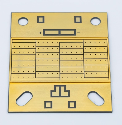
Ceramic materials achieve unique physical properties. Aluminum Oxide, Aluminum Nitride, and Silicon Nitride succeed where pure metals fail. They offer simultaneous high thermal conductivity and absolute electrical insulation. A well-designed 3D Ceramic Packaging Substrate bypasses standard encapsulation limits. It provides direct, highly engineered avenues for heat dissipation.
Integration of Through‑substrate via (TSV) ceramic technology transforms structural package design. Designers engineer precise, vertical metalized pathways directly into the ceramic block. These vias bypass insulating layers entirely. They act as direct thermal bridges. Heat flows from the hottest active zones continuously.
The routing process follows a highly specific physical path:
Heat generates at the active semiconductor junction during switching.
Thermal energy travels laterally a very short distance.
The energy enters the customized vertical metalized via.
The high-conductivity channel pulls heat straight through the ceramic body.
Heat dissipates safely into the primary system heat sink.
You eliminate the trapped inter-layer heat completely. We rely on these vias to prevent localized hotspot pooling.
Ceramics possess a remarkably high Young’s modulus. They provide absolute mechanical rigidity under stress. Their Coefficient of Thermal Expansion (CTE) aligns closely with semiconductor materials. Silicon and wide-bandgap materials expand predictably when heated. Ceramics match this specific expansion rate.
This harmony prevents severe physical warping. It stops interface delamination during extreme thermal cycling. Die-cracking becomes practically non-existent. Polymer alternatives warp heavily under identical stress profiles. You protect delicate silicon structures by providing a stable, unyielding foundation. The industry recognizes this structural stability as a primary reliability mechanism.
Selecting the right ceramic requires careful calculation. You must balance absolute thermal limits against manufacturing complexity. Budget constraints also dictate material viability. Not every application requires top-tier performance.
Aluminum Oxide serves as the industry workhorse. It delivers moderate thermal conductivity. Performance typically ranges between 24 and 30 W/m·K. It maintains excellent electrical insulation. We use it frequently for medium-power applications. It excels where hermeticity and mechanical stability matter most. You avoid the extreme premium costs associated with advanced nitrides.
Aluminum Nitride handles exceptional heat loads. It delivers outstanding thermal conductivity. Performance ranges from 170 to 230 W/m·K. It reduces package thermal resistance drastically compared to standard lead frames. However, severe trade-offs exist. The material requires extremely high sintering temperatures. Processing often exceeds 1800°C. It requires highly complex machining techniques. Consequently, it typically carries a 5 to 10x cost multiplier over baseline Al₂O₃.
Silicon Nitride offers best-in-class physical resilience. It dominates in fracture toughness metrics. It handles severe thermal shock perfectly. The automotive sector increasingly adopts it as the standard. Electric Vehicle (EV) traction inverters utilize heavy SiC modules. These modules face harsh physical vibrations and rapid thermal cycling. Si₃N₄ survives these brutal conditions without micro-fracturing.
| Material Type | Thermal Conductivity (W/m·K) | Primary Strength | Ideal Application |
|---|---|---|---|
| Aluminum Oxide (Al₂O₃) | 24 - 30 | Cost-effective hermeticity | Medium-power industrial sensors |
| Aluminum Nitride (AlN) | 170 - 230 | Maximum heat dissipation | High-density 3D ICs, Optoelectronics |
| Silicon Nitride (Si₃N₄) | 80 - 90 | Extreme fracture toughness | EV traction inverters, Automotive |
Ceramic packaging remains an over-engineered solution for cheap consumer electronics. You incur unnecessary costs using it for low-power gadgets. However, it represents a mission-critical necessity for several advanced verticals. Let us explore the deployment environments requiring these robust materials.
| Application Sector | Critical Constraint | Ceramic Solution |
|---|---|---|
| Power Electronics | High Voltage & Thermal Cycling | Si₃N₄ AMB Substrates |
| Telecommunications | Moisture Intrusion & Frequency Drift | Al₂O₃ Hermetic Packages |
| Optoelectronics | Complex 3D Routing & Heat Density | AlN Multi-layer Structures |
Deploying modern 800V infrastructures requires robust silicon carbide (SiC) components. These components handle extreme, sudden heat loads. Standard substrates delaminate under these rapid temperature spikes. Si₃N₄ Active Metal Brazed (AMB) substrates prevent these thermal bottlenecks entirely. They extend the component lifecycle significantly. Furthermore, they reduce internal cooling system overhead. You gain operational efficiency immediately.
High-frequency signals degrade heavily when moisture enters a package. Environmental humidity alters dielectric properties quickly. Ceramics provide true, uncompromising hermetic sealing. They maintain highly stable impedance. They prevent the moisture absorption completely inherent to standard epoxy packages. Network operators rely on this stability for outdoor cell tower deployments.
Laser diodes generate massive heat within microscopically small footprints. Complex sensor arrays require highly customized 3D routing. They also require internal cavity structures for optical alignment. Multi-layer co-fired ceramic processes support these custom geometries natively. You can integrate complex wire bonds and thermal vias securely into one solid component.
A premium 3D package will easily underperform under poor system design. Surrounding thermal architecture must be flawless. Flawed heat sinks negate material conductivity benefits. You must employ active system-level mitigation strategies.
Thermal analysis cannot remain a post-design validation step. It must occur early. You must embed it in the architectural exploration phase. Engineers rely heavily on Finite Element Analysis (FEA) for thermal flow predictions. Identify specific die stacking orders early. Map out hotspot overlaps before you commit to any substrate layout. Failing to model these overlaps guarantees thermal throttling. You save massive redesign costs by modeling physical heat flows first.
The bond between your active chip and the ceramic surface dictates everything. It often dictates the overall system thermal limit. Standard pastes degrade and pump out over time. Evaluate advanced TIMs carefully. Nano-structured metals perform exceptionally well. Aligned carbon nanotubes also provide incredible interface conductivity. Ensure your interface material does not throttle the substrate’s inherent heat-wicking capabilities. A poor TIM renders an expensive AlN substrate completely useless.
3D ceramic substrates operate as a strategic enablement tool. They are strictly vital for next-generation power and density scaling. They are never just a passive structural component. They actively solve 3D integration thermal bottlenecks.
Teams should base their material selection entirely on hard data. Evaluate Al₂O₃, AlN, or Si₃N₄ based on strict thermal resistance (Rthjc) requirements. Prioritize long-term thermal cycling thresholds rather than just initial component cost.
Initiate joint simulation phases immediately. Begin prototyping with specialized substrate manufacturers early in the design cycle. Validate your CTE compatibility thoroughly. Finalize your internal via routing layouts using advanced FEA modeling tools before finalizing any silicon design.
A: In 3D ICs, dies are stacked vertically. Heat generated by a middle or top layer must physically conduct through other active, heat-generating layers to escape. This architectural reality compounds the temperature across all interfaces, trapping heat inside the package.
A: For moderate power applications, advanced lead frames offer excellent cost-to-performance ratios. However, because they require insulating polymer layers (which act as thermal barriers), they cannot match the continuous, high-conductivity paths provided by ceramics in extreme heat-flux environments.
A: TSVs act as direct thermal short-circuits. By filling vertical channels with high-conductivity metals, they bypass layers of higher thermal resistance. This pulls heat directly from the active die down to the board or heat sink efficiently.
A: Not necessarily. While AlN has the highest thermal conductivity, it is brittle and expensive. For environments involving severe mechanical shock or continuous rapid temperature cycling (like automotive), Silicon Nitride (Si₃N₄) is often preferred for its superior fracture toughness.


