


Views: 0 Author: Site Editor Publish Time: 2026-05-29 Origin: Site


Semiconductor architectures now push toward extreme power densities and complex heterogenous integration. As a result, traditional organic substrates frequently fail to meet strict thermal and hermetic requirements. Standard plastics and resins simply warp, blister, or crack under intense operational loads.
Engineering teams frequently hit the thermal or frequency ceilings of these conventional materials. When this happens, transitioning to a 3D Ceramic Packaging Substrate is no longer optional. It becomes a baseline reliability requirement. High-performance modules demand a physical foundation capable of surviving harsh conditions without degrading over time.
This guide bypasses basic, surface-level definitions. Instead, we examine the exact engineering applications where 3D ceramic configurations justify their higher initial procurement costs. You will learn how these advanced materials deliver extreme environment survivability and enable complex multi-layer routing for next-generation electronics.
3D ceramic substrates are mission-critical for applications where CTE (Coefficient of Thermal Expansion) mismatch causes thermal fatigue in standard substrates.
The primary beneficiaries include Electric Vehicle (EV) power modules, high-frequency 5G/6G telecom arrays, and hermetically sealed aerospace sensors.
Evaluating these substrates requires trading off thermal conductivity against electrical routing precision (e.g., HTCC vs. LTCC methodologies).
Supplier capability in managing co-firing shrinkage tolerances (often demanding < ± 0.1%) is the primary risk factor during procurement.
Standard 2D substrates and organic resins suffer heavily in harsh industrial environments. They face rapid thermal degradation, moisture ingress, and mechanical failure when exposed to extreme vibration or heat cycling. When a standard PCB approaches 150°C, the resin matrix often begins to soften. This leads to warped boards and broken solder joints.
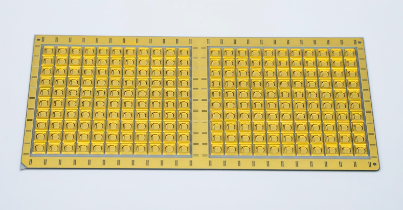
To solve this, engineers turn to fine ceramics. Materials like Alumina, Aluminum Nitride, and Silicon Nitride can be molded with sophisticated 3D internal routing. They feature stepped cavities and blind vias. This creates a three-dimensional protective and functional envelope around sensitive bare dies.
You should base your core evaluation on three feature-to-outcome criteria:
CTE Matching: Ceramics closely match the thermal expansion rates of silicon and silicon carbide (SiC) bare dies. This prevents delamination during severe thermal cycling.
True Hermeticity: Near-zero porosity prevents moisture and oxygen degradation. Standard moisture ingress can reduce chip lifespans from 100,000 hours to mere thousands. True hermetic seals block this entirely.
3D Spatial Efficiency: Multi-layer co-fired structures allow for micro-channels, embedded passives, and recessed cavities. These features slash the overall device footprint significantly.
Power electronics represent one of the most demanding environments for substrate materials. The primary success criterion here is managing the intense heat generated by wide-bandgap semiconductors. Chips like SiC and GaN run incredibly hot. You must dissipate this heat without sacrificing the lifespan of the power module.
In traditional setups, Aluminum-DBC (Direct Bonded Copper) substrates handle EV traction inverters. However, these substrates often experience micro-cracking under the rapid heating and cooling cycles of EV fast charging. As the automotive industry shifts toward 800V architectures, DBC micro-cracking becomes a critical failure point.
Switching to a modern ceramic solution creates a measurable impact. Engineers typically move to Silicon Nitride (Si3N4) via Active Metal Brazing (AMB). This drastically increases thermal cycling durability. Furthermore, advanced 3D designs allow for integrated cooling channels directly within the substrate body. These micro-channels lower hotspot temperatures by measurable margins. Frequently, engineering teams record 12°C to 20°C temperature drops, extending the inverter’s operational life.
| Substrate Type | Thermal Conductivity | Mechanical Toughness | Thermal Cycling Lifespan |
|---|---|---|---|
| Standard Aluminum-DBC | Moderate (20-30 W/m·K) | Low (Prone to cracking) | Below 10,000 cycles |
| Aluminum Nitride (AlN) | High (170+ W/m·K) | Moderate (Brittle under shock) | Up to 50,000 cycles |
| Silicon Nitride (Si3N4) AMB | Good (90 W/m·K) | Extremely High | 100,000+ cycles |
Telecommunication infrastructure faces an entirely different set of physics problems. The core success criteria involve minimizing signal attenuation, dielectric loss, and electromagnetic interference (EMI) at millimeter-wave frequencies. If you lose signal strength at the board level, your entire network array suffers.
Standard PCBs struggle with excessive signal loss at these higher frequencies. Telecommunication hardware requires a High‑frequency ceramic substrate capable of dense, three-dimensional RF routing without crosstalk. FR4 materials absorb too much signal energy above 10 GHz.
Low Temperature Co-fired Ceramic (LTCC) technology solves this issue beautifully. Because it uses lower sintering temperatures (850–900°C), manufacturers can use highly conductive metals like gold, silver, and copper. This differs from high-temperature ceramics that restrict you to less conductive refractory metals. LTCC provides an ultra-low dielectric loss tangent (low-tanδ). It acts as the industry standard for high-frequency antenna-in-package (AiP) modules, optical transceivers, and automotive radar systems.
Space-bound and military hardware demand uncompromising reliability. They operate under ionizing radiation, extreme temperature fluctuations, and high-G mechanical shock. You must design for absolute environmental isolation while facing strict weight and volume constraints.
Traditional packaging simply takes up too much physical space or fails in vacuums. Advanced 3D ceramics offer two distinct design impacts for high-reliability sensors:
First, they enable highly complex stepped cavities. 3D manufacturing allows engineers to build recessed physical tiers inside the package. This staggered layout allows ultra-fine pitch wire bonding (e.g., 40-micron spacing) without risk. You can separate the wires physically across different vertical levels, preventing short circuits in tight spatial constraints.
Second, they create ultra-thin sensor packages. Advanced multilayer ceramics can compress complete protective enclosures for magnetic or radiation sensors. Some designs shrink down to sub-300-micron total thicknesses. This incredible reduction enables deployment in highly restrictive areas, such as the tiny gaps between motor stators and rotors.
Buyers must match the manufacturing process to their specific thermal and electrical priorities. You cannot buy a universal ceramic substrate. You must weigh the tradeoffs carefully.
Manufacturers sinter HTCC at roughly 1600°C. This extreme heat provides exceptional thermal conductivity and mechanical strength. However, the high temperature limits metallization to refractory metals like tungsten or molybdenum. These metals possess lower electrical conductivity. HTCC works best for extreme high-temp, high-power environments where signal speed is secondary.
LTCC mixes ceramic with glass frit to lower the sintering point to 900°C. This allows excellent electrical performance with high-conductivity metals like gold and silver. It also grants high 3D design freedom for embedded components. The major drawback is lower thermal conductivity compared to HTCC (often 2–7 W/m·K due to the added glass). It fits best for RF, telecom, and complex sensor arrays.
| Material Type | Primary Characteristic | Best Application Use Case |
|---|---|---|
| Alumina (Al2O3) | Cost-effective, versatile baseline performance. | General LED lighting, standard automotive modules. |
| Aluminum Nitride (AlN) | Premium thermal management (>170 W/m·K). | High-power lasers, dense power grids. |
| Silicon Nitride (Si3N4) | The undisputed leader for mechanical toughness. | EV traction inverters, high-shock military gear. |
Transitioning to 3D ceramics requires rigorous supplier vetting. Many manufacturers claim ceramic capabilities, but few possess the precise metrology and yield control required for 3D multilayer co-firing. Small defects lead to massive field failures. You must audit your vendors strictly.
Use the following logic to shortlist potential suppliers:
Shrinkage Control Tolerance: Ask if the supplier can maintain shrinkage tolerances below ±0.1% during co-firing. Ceramics shrink significantly when baked. Poor control leads to layer delamination and via misalignment.
Via Density and Metallization Resolution: Verify the supplier's screen printing or photolithography limits. You need to know their minimum line width and spacing limits to ensure they can handle your complex designs.
Testing and Compliance Capability: Do they test in-house? Ensure they possess capabilities for thermal shock testing (JEDEC standards), hermetic leak testing (Helium fine leak), and acoustic microscopy for hidden void detection.
Next-Step Prototype Actions: Never commit to high-volume tooling immediately. Request prototype runs using Multilayer Sintered 3D Ceramic (MSC) or additive manufacturing (3D printed ceramics). Validate your cavity designs mechanically and thermally first.
Advanced 3D ceramic packaging substrates do not serve as a universal replacement for standard printed circuit boards. Instead, they act as the definitive solution for rigorous applications. When thermal fatigue, high-frequency signal integrity, and absolute hermeticity dictate your product's viability, ceramics are your safest path forward.
Engineering teams facing repeated field failures in harsh environments should act now. You should initiate a thermal and structural simulation comparing your current organic substrates against robust AlN or Si3N4 ceramic alternatives. Securing the right substrate configuration ensures long-term reliability and shields your hardware from preventable environmental degradation.
A: Ceramics require significantly higher upfront tooling and raw material costs than FR4. However, they offset these initial expenses by delivering vastly longer lifespans in harsh environments. This extended durability prevents frequent field failures, thereby reducing warranty replacements and overall maintenance demands dramatically.
A: Yes. Emerging additive manufacturing techniques, such as 3D printing of technical ceramics, have lowered the barrier for rapid prototyping. These technologies allow engineering teams to test complex internal structures and micro-channels quickly without paying for expensive initial mold investments.
A: It uses specific glass-ceramic blends, such as LTCC, that provide a very low dielectric constant and an ultra-low loss tangent. Manufacturers combine this stable base with highly conductive gold or silver trace routing. This powerful combination minimizes electrical resistance and prevents signal degradation at high gigahertz bands.


