

Views: 0 Author: Site Editor Publish Time: 2026-09-25 Origin: Site


The rapid expansion of the ultraviolet A market is driven heavily by demanding applications like industrial curing, high-resolution 3D printing, and precision gas sensing. However, this growth has exposed a critical engineering bottleneck. As manufacturers relentlessly push for higher irradiance levels, managing extreme localized heat while maximizing photon output in increasingly miniaturized footprints is pushing traditional materials past their breaking point.
Standard organic packaging resins and plastic lead frames simply cannot survive this harsh environment. They degrade rapidly under intense UV photon bombardment, leading to severe color shifts, diminished optical output, and ultimately, catastrophic diode failure. To overcome these physical limitations, the industry is transitioning toward fully engineered inorganic solutions. By combining Direct Plated Copper technology with a three-dimensional cavity design, advanced ceramic bases provide the ultimate foundation for high-wattage UV systems. This comprehensive guide explores the mechanics of copper metallization, the distinct advantages of specialized cavity structures, and why upgrading your packaging architecture is critical for long-term operational success.
Superior Heat Dissipation: Aluminum Nitride ceramics paired with direct copper metallization offer unmatched thermal conductivity, drastically extending the lifespan of high-power diodes.
Enhanced Light Extraction: Engineered cavity structures act as precise micro-reflectors, bouncing side-emitted light outward to significantly boost optical efficiency.
Exceptional Durability: Entirely inorganic architectures are completely immune to radiation degradation, preventing the yellowing and cracking that plague traditional organic encapsulants.
High-Density Integration: Advanced photolithography enables ultra-fine circuit resolution, allowing engineers to design highly compact, densely packed diode arrays.
Engineers designing high-intensity optical systems face a unique set of material limitations. The spectrum ranging from 365nm to 395nm generates environmental stressors that standard visible-light components never encounter on the field.
Industrial diodes are notorious for their brutal thermal profiles. While standard visible lighting runs relatively cool, a typical high-power semiconductor chip converts only about 30 to 40 percent of its electrical input into usable light. The remaining energy instantly transforms into intense, localized heat. When a dense 10-watt array powers up, the junction temperature can skyrocket within milliseconds.
If this thermal load is not rapidly wicked away from the die, the consequences are immediate and severe. Forward voltage drops, overall radiant flux decreases, and the emitted wavelength begins to shift upward. In precision applications like semiconductor lithography or chemical curing, even a microscopic 3nm wavelength drift can render the entire curing process completely ineffective.
Beyond thermal management, material degradation remains a massive hurdle. Legacy materials such as epoxy resins, silicones, and plastic-molded lead frames are highly vulnerable to high-energy photon bombardment. Continuous exposure to intense radiation breaks down the molecular bonds within these organic polymers through a destructive process known as chain scission.
As the encapsulation degrades, it turns a cloudy yellow or dark brown, actively absorbing the very light the diode is trying to emit. Eventually, the embrittled material cracks, exposing the delicate semiconductor to moisture and oxygen. Directing scattered light without losing intensity requires robust, zero-degradation UVA LED packaging capable of withstanding years of continuous, high-stress operation.
Recent market analyses reveal a massive migration away from silicone and epoxy encapsulants across the sub-400nm spectrum. As industrial curing systems push for irradiance levels exceeding 20 watts per square centimeter, organic materials simply burn out. Market intelligence indicates that integrating three-dimensional metallized cavities is no longer a premium feature. It has become the absolute baseline requirement for top-tier UV system manufacturers aiming for 20,000-hour operational lifespans and zero-maintenance guarantees. This definitive shift underscores a broader industry reality where thermal-mechanical reliability now entirely dictates market dominance.
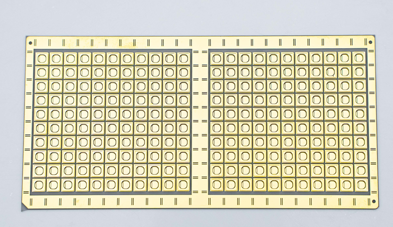
To eliminate the vulnerabilities of organic plastics, tier-one manufacturers have shifted toward advanced inorganic architectures. At the core of this technological leap is the monolithic three-dimensional ceramic package.
In legacy electronic manufacturing, a base board is usually flat and two-dimensional. Any required reflective cups or retaining walls must be manufactured separately and glued onto the base using organic adhesives. Unfortunately, these glue lines become the weakest link, highly vulnerable to the same thermal stress and decay mentioned earlier.
A monolithic 3D architecture completely eliminates this weak link. Instead of gluing a separate reflector ring, the raised perimeter wall is inherently built into the ceramic base itself. Because there are no organic adhesives in the optical path, the integrated housing provides a structurally sound, hermetic environment for the semiconductor.
This specific architecture is precisely tailored for extreme environments and consists of three primary elements working in unison. The foundational ceramic base provides rigid structural support and the primary thermal dissipation pathway. Directly bonded to this base is the copper metallization layer, which handles complex electrical routing. Finally, the raised perimeter wall surrounds the chip cavity, creating a protective micro-environment that isolates the die from mechanical shear stress while establishing a physical mount for quartz lenses.
The method utilized to bond the electrical circuitry to the base is just as vital as the material itself. Direct Plated Copper has emerged as the premier manufacturing standard for high-performance optical modules.
Unlike older methods that rely on thick, thermally restrictive adhesives, a DPC ceramic substrate bonds copper directly to the base at a molecular level. The process begins in a vacuum chamber, where magnetron sputtering deposits a microscopic titanium bonding layer and a thin copper seed layer onto the bare ceramic. Following this, advanced semiconductor-grade photolithography defines the exact circuit pattern. Finally, electroplating grows the copper to the required thickness, often ranging from 10 to 100 micrometers. This creates an uninterrupted thermal bridge from the chip directly to the heat sink.
When engineering miniaturized modules, this modern plating technology offers distinct advantages over legacy Direct Bonded Copper or Low-Temperature Co-fired Ceramics.
Because legacy bonding relies on high-temperature oxidation to fuse thick copper foils, it severely limits etching precision. In stark contrast, modern photolithography achieves ultra-fine line widths and spacing down to 30 micrometers. This incredible resolution allows engineers to pack more diode chips into a significantly smaller footprint without the risk of electrical shorting. Furthermore, because the plating is a low-temperature process, it minimizes residual thermal stress, preventing the board from warping during rapid heating and cooling cycles on the assembly line.
While the flat metallized base handles electrical routing and heat transfer, the elevated three-dimensional elements are dedicated entirely to optical optimization.
A bare diode chip emits light in all directions, including out of its sides. In a flat package, these lateral photons are often absorbed by surrounding components and lost entirely as heat. The angled walls of the ceramic dam structure are specifically engineered to solve this exact problem. By applying a highly reflective metallic coating, such as silver or specialized aluminum alloys, to the inner cavity walls, side-emitted light is captured and bounced forward. This precise micro-reflector effect significantly maximizes Light Extraction Efficiency, ensuring every available photon reaches the target surface.
Because standard silicones degrade rapidly, high-power arrays require inorganic lenses made of specialized transmitting glass or quartz. The integrated cavity provides a rigid, perfectly dimensioned housing for these optics. The elevated walls ensure precise focal alignment, holding the quartz lens at the exact optimal distance from the semiconductor die. This seamless integration also creates a hermetically sealable environment, protecting delicate wire bonds from external moisture and mechanical shock.
At the heart of the package is the material itself. For high-wattage industrial applications, the choice of base material dictates the absolute thermal ceiling of the entire system.
Alumina is highly cost-effective and perfectly suitable for low-power indicator lights, offering a thermal conductivity of roughly 24 to 30 watts per meter-kelvin. However, this is woefully inadequate for dense array systems.
When driving currents exceed 1000 milliamps, an AlN ceramic substrate becomes an absolute necessity. Aluminum Nitride boasts a phenomenal thermal conductivity ranging from 170 to 230 watts per meter-kelvin, which is nearly seven to ten times higher than Alumina. This ensures that the massive thermal load generated by the diode is instantly wicked away, keeping the junction temperature well within safe operating limits and preventing catastrophic burnout.
Thermal-mechanical stability is just as critical as raw heat dissipation. As a module powers on and off, materials expand and contract. Most high-power chips are built on Gallium Nitride or Silicon Carbide wafers, which have a thermal expansion coefficient of approximately 4.0 to 5.5 parts per million per kelvin. Aluminum Nitride sits perfectly within this range at roughly 4.5 parts per million per kelvin. This exact synchronization eliminates solder joint fatigue and prevents microscopic cracks in the die during rapid thermal cycling.
To justify the return on investment for advanced packaging, engineering and procurement teams must evaluate the total lifecycle of the component. Below is a direct technical comparison.
| Technical Metric | Traditional Plastic Lead Frame | 3D DPC Ceramic Architecture |
|---|---|---|
| Thermal Conductivity | Low to Moderate. Heat is bottlenecked by polymer layers. | Extremely High. 170-230 W/m·K direct thermal path. |
| UV Degradation Resistance | Poor. Resins yellow and crack under high irradiance. | Excellent. 100% inorganic materials are immune to decay. |
| Circuit Resolution | Standard etching limits density. | Ultra-fine. Down to 30μm line width/spacing. |
| Total Cost of Ownership | High maintenance due to frequent module replacements. | Highly cost-effective over long-term continuous operation. |
While engineered ceramics carry a higher initial unit cost, the total cost of ownership heavily favors them for commercial deployments. Traditional organic packages suffer from rapid aging, leading to frequent module replacements, machine downtime, and expensive warranty claims. Because inorganic materials are immune to decay, they offer a lifespan up to ten times longer than legacy alternatives. For industrial end-users, this translates to massive cost savings in maintenance and uninterrupted production cycles.
The combination of extreme thermal stability and precise optical control makes these components the backbone of several demanding high-tech industries.
In the manufacturing sector, roll-to-roll printing lines and automated assembly systems rely on high-intensity light to cure inks, coatings, and heavy-duty adhesives. These machines require sustained, peak-power output. The superior heat dissipation of Aluminum Nitride allows these curing arrays to operate continuously without thermal degradation, ensuring fast and consistent chemical cross-linking.
Resin-based 3D printing and semiconductor lithography depend heavily on 365nm to 405nm wavelengths. These precision applications require uniform light distribution and absolute wavelength stability. The integrated dam structure guarantees that quartz lenses remain perfectly aligned, while the extreme thermal stability prevents wavelength drift, ensuring printed micro-structures maintain exact dimensional accuracy.
Integrating these advanced components into next-generation products requires selecting a partner capable of precise execution and rigorous quality control.
Direct Plated Copper technology requires strict environmental controls. Engineering buyers should prioritize vendors with mature vacuum sputtering equipment and robust electroplating lines. You must verify their line width resolution and copper thickness limits. A reliable manufacturer will consistently achieve sub-50 micrometer line spacing, preventing electrical shorts in highly compact arrays, while maintaining exceptional copper-to-ceramic peel strength.
Off-the-shelf flat boards are rarely sufficient for optimized optical systems. It is vital to partner with a supplier who can engineer a custom high power LED substrate tailored specifically to your lens geometry. The manufacturer must be able to adjust the cavity angle for maximum reflection, customize the depth to match the focal point of your quartz lenses, and apply precise reflective metallization to the inner walls. Testing prototype samples for exact focal alignment is a critical engineering step before committing to mass production.
As industrial optical systems continue to push higher wattages, traditional organic packaging is no longer a viable option. The extreme heat and intense radiation demand a much more robust solution. Upgrading to a three-dimensional ceramic packaging architecture combines the ultra-fine circuit precision of modern plating technology with the unmatched thermal conductivity of Aluminum Nitride. Furthermore, the customized cavity design maximizes optical output while protecting the delicate semiconductor from environmental stress. If your current modules suffer from premature thermal degradation or unacceptable color shifts, it is time to upgrade your foundation. Evaluate your specific thermal loads and visit XR MKPCB to explore custom 3D ceramic solutions tailored for your next-generation systems.
Direct Bonded Copper involves extreme melting temperatures, making it difficult to create precise three-dimensional shapes without inducing severe thermal stress. Direct Plated Copper uses vacuum sputtering at much lower temperatures. This allows for incredibly thin, precise copper layers and ultra-fine circuit resolution, which is absolutely critical for densely packed diode arrays.
No, a properly engineered cavity does the exact opposite. Because semiconductor chips emit light from their sides as well as their top, side emissions are often lost in flat packages. The angled, metallized walls act as precise micro-reflectors, capturing those lateral photons and bouncing them forward to significantly increase overall optical efficiency.
The necessity depends entirely on the power output. For low-power indicators that generate manageable heat, Alumina is often sufficient and cost-effective. However, industrial high-power arrays produce intense thermal loads. In these demanding scenarios, Aluminum Nitride is mandatory because it transfers heat up to seven times faster than Alumina, preventing dangerous wavelength shifting and diode failure.
Yes, advanced manufacturing allows for deep structural customization. Engineers can adjust the wall height, inner angle, and cavity footprint to perfectly accommodate specific flat glass or dome quartz lenses. This ensures the lens stays perfectly aligned at the correct focal length while providing a secure physical housing.
Because inorganic materials like Aluminum Nitride and plated copper do not suffer from chain scission or UV-induced yellowing, their operational lifespan is vastly superior to organic resins. When properly heat-sinked, these engineered modules can easily exceed 20,000 to 30,000 hours of continuous operation without significant optical decay.
The expansion coefficient measures how much a material expands when heated. If the chip and the base expand at different rates during operation, it creates severe mechanical shear stress that can crack solder joints or fracture the die itself. Engineered ceramics closely match the expansion rate of semiconductor chips, preventing stress during rapid thermal cycling and drastically improving long-term reliability.


