


Views: 0 Author: Site Editor Publish Time: 2026-05-22 Origin: Site


As power densities surge in modern electronics, engineers face a critical bottleneck. You must manage escalating thermal loads inside increasingly shrinking footprint constraints. High-power devices and complex heterogeneous integration push conventional materials entirely beyond their safe operational limits. Transitioning from standard organic boards to a 3D Ceramic Packaging Substrate represents a major structural shift. The specific manufacturing methodology your supplier uses directly controls system-level reliability. It dictates high-frequency RF performance and governs absolute heat dissipation limits. Understanding how these materials are built is absolutely essential. It empowers you to accurately evaluate supplier capabilities before committing to a design. You can anticipate hidden yield risks early in your development cycle. Ultimately, grasping these precise manufacturing nuances ensures you select the correct technology for seamless, high-volume production.
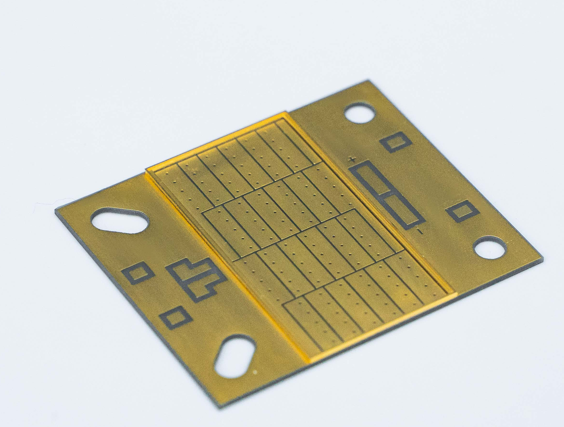
Manufacturing a 3D ceramic packaging substrate relies on precision layer-by-layer fabrication, typically involving tape casting, micro-via punching, precision metallization, and co-firing.
Process selection (HTCC, LTCC, or DPC) dictates the final capabilities of the thermal management substrate, requiring strict alignment with target thermal and electrical specifications.
Evaluating a manufacturing partner requires looking beyond theoretical specs to assess yield rates, shrinkage control, and automated quality assurance standards.
Scaling from prototype to production carries specific tooling and lead-time risks that must be factored into project timelines.
Many engineering teams initially default to traditional FR4 materials for printed circuit boards. However, these organic boards quickly fail under extreme operational stress. They suffer from rapid structural degradation when exposed to prolonged high temperatures. Signal loss becomes unacceptable at high frequencies due to poor dielectric characteristics. Furthermore, a mismatched coefficient of thermal expansion (CTE) severely stresses delicate solder joints during rapid temperature cycling. Moisture absorption in standard laminates also degrades long-term isolation resistance.
Upgrading to a dedicated Thermal management substrate solves these core physical limitations. A successful transition yields measurable technical victories across the board. You gain guaranteed hermeticity for sensitive bare silicon dies. You secure superior dielectric properties for immaculate RF signal integrity. Devices achieve highly stable operation in the harshest environments conceivable. Aerospace phased arrays, automotive EV power traction modules, high-power LED matrices, and advanced radar transmitters all rely strictly on this stability.
Naturally, ceramic components carry a higher upfront unit cost compared to organic laminates. You must balance this initial expense against profound operational benefits. Upgrading substantially improves device longevity in the field. It often eliminates the need for secondary heat sinks or complex liquid cooling loops. This direct reduction in thermal management overhead justifies the initial material investment without requiring complex financial justifications. The component survives longer, performs better, and simplifies your external mechanical assembly.
Fabricating these complex structures requires immense mechanical and chemical precision. The process relies on sequential, carefully monitored stages. Any deviation in early steps cascades into catastrophic failures later.
Slurry Preparation & Tape Casting: Manufacturers begin by formulating specialized ceramic powders. They typically use high-purity Alumina or Aluminum Nitride. Technicians mix these mineral powders alongside organic binders, dispersants, and plasticizers. This creates a highly homogeneous liquid slurry. The factory then casts this mixture onto a moving carrier film. As it dries, it forms highly uniform "green" tapes. These unfired sheets remain flexible and ready for mechanical processing.
Micro-Via Formation: Vertical interconnect access dictates modern 3D architecture success. Factories use mechanical punching or laser drilling to create thousands of tiny vias. Mechanical punches work exceptionally well for standard grid layouts. Laser drilling handles ultra-fine pitches and complex geometries. These vertical holes eventually connect different layers electrically.
Metallization & Circuit Patterning: Next, automated machines screen-print conductive metal pastes onto the green tape. High-temperature processes require robust refractory metals like tungsten or molybdenum. Low-temperature processes use highly conductive silver, gold, or copper. The paste fills the tiny micro-vias and forms complex, customized circuit patterns across the surface.
Stacking & Lamination: Operators then meticulously align multiple functionalized layers. They stack them into a monolithic 3D structure using optical alignment tools. The lamination press applies high isostatic pressure alongside carefully controlled temperatures. This binds the distinct sheets into a single, cohesive block before firing.
Sintering (Co-firing): The final primary step involves extreme heat inside a specialized kiln. The initial heating phase burns out all organic binders safely. The subsequent peak temperature densifies the ceramic particles and metal traces simultaneously. Engineers must execute a mathematically precise thermal profile. Strict shrinkage control during this densification phase separates premium manufacturers from mediocre ones.
You must align your selected manufacturing process to your specific application. Three dominant technologies define the modern market. Each carries distinct advantages and strict operational limitations.
HTCC undergoes firing at temperatures exceeding 1500°C. This extreme heat mandates the use of refractory metals for conductive traces. The outcomes include maximum structural integrity and exceptional thermal endurance. HTCC remains the absolute gold standard for extreme hermetic packaging. Defense contractors and deep-space engineers heavily rely on this robust technology.
LTCC fires at much lower temperatures, typically below 900°C. This lower thermal threshold allows manufacturers to use highly conductive metals. You can implement silver, gold, or copper traces seamlessly. The primary outcome is superior high-frequency RF performance. It enables complex 3D passive component integration for telecommunications. However, it trades away some absolute thermal conductivity compared to HTCC.
DPC utilizes advanced thin-film metallization techniques. The factory applies copper to pre-fired ceramic bases using sputtering and electroplating. This delivers exceptional precision for fine-pitch routing. It excels in high heat flux applications where thermal bottlenecks destroy components. Engineers typically use DPC for specialized 2.5D or 3D surface integrations, especially in high-power UV LEDs and automotive LiDAR systems.
| Technology Type | Firing Temperature | Typical Metallization | Primary Advantage | Ideal Application |
|---|---|---|---|---|
| HTCC | > 1500°C | Tungsten, Molybdenum | Maximum mechanical strength & hermeticity | Aerospace, harsh environment sensors |
| LTCC | < 900°C | Silver, Gold, Copper | Excellent RF performance & low signal loss | 5G telecom, radar modules |
| DPC | Pre-fired substrate | Plated Copper | High heat flux & ultra-fine trace routing | High-power LEDs, power modules |
Moving from a theoretical CAD design to a physical product involves distinct manufacturing risks. You must anticipate these hurdles early to avoid costly redesigns.
Ceramic tapes shrink significantly during the sintering process. X-Y-Z axis shrinkage typically ranges between 12% and 20%. Manufacturing maturity dictates the exact tolerance control achieved. High-density interconnects demand perfect layer-to-layer alignment. Poor shrinkage control guarantees internal short circuits or broken via connections. Experienced vendors utilize advanced predictive modeling to compensate for this shrinkage during the initial stencil design.
Physical deformation severely threatens yields during cooling phases. This risk scales dramatically when using larger substrate panels. Highly asymmetric copper-to-ceramic ratios also induce severe bowing due to differing contraction rates. Proper cooling profiles mitigate this structural warpage. If a board warps beyond specified limits, automated pick-and-place machines cannot populate it later.
Metallization delamination remains a primary failure mode under heavy thermal cycling. You must specify rigorous pre-production testing to validate the process. Shear strength evaluations and thermal shock cycles confirm bond integrity. Weak adhesion inevitably leads to catastrophic field failures when the device powers up and heats rapidly.
Scaling up requires custom mechanical assets. Be completely transparent about tooling lead times. Custom via-punching tools and specific screen-printing masks take significant time to fabricate. These physical assets directly impact your critical time-to-market. Failing to account for tooling delays often derails entire product launch schedules.
Designing routing paths based on standard FR4 PCB rules instead of ceramic-specific shrinkage tolerances.
Ignoring asymmetric copper balancing across layers, leading to severe board warpage.
Failing to specify thermal shock testing criteria before approving the first article prototype.
Choosing a vendor requires aggressive technical vetting. You must look far beyond glossy brochures and theoretical capabilities.
Always demand historical defect rates from prospective partners. Ask for statistical process control (SPC) data covering similar layer-count substrates. Theoretical capabilities matter very little if the factory struggles to produce them consistently. A competent vendor will happily share their Cpk (process capability index) data for critical dimensions.
Evaluate the vendor's raw material supply chain. Do they formulate custom slurries in-house? Do they rely entirely on third-party green tapes? In-house formulation offers immense customization flexibility. It allows them to tweak dielectric constants or thermal conductivity for your specific needs. It also substantially bolsters supply chain security against external market disruptions.
Strict industries require flawless paperwork and validation. Verify critical certifications immediately. Look for ISO 9001 as a mandatory baseline. Demand IATF 16949 for any automotive projects. Require MIL-PRF-38534 for defense and aerospace contracts. Furthermore, inspect their in-house testing laboratory. They absolutely need Scanning Acoustic Microscopy (SAM) to detect internal voids. They require X-Ray inspection for via alignment and dedicated hermeticity testing bays.
Assess the vendor's actual production floor layout. Can they scale seamlessly from low-volume quick-turn prototyping to automated, high-volume runs? Transferring a complex product to a completely different facility mid-stream introduces massive redesign risks. You want a partner who can handle the initial engineering batches and the eventual mass production under one robust quality management system.
Audit the prospective factory personally whenever possible.
Observe their cleanroom disciplines directly.
Review their automated optical inspection (AOI) parameter limits.
Ask operators on the floor how they handle non-conforming material.
The intricate manufacturing process directly dictates your final device performance. Every phase, from initial tape casting to final high-temperature sintering, introduces strict physical variables. Evaluating these advanced materials is fundamentally an exercise in precise matching. You must align specific co-firing or plating technologies directly to your anticipated operational loads.
Do not wait until the final design phase to consider your substrate options. Engage your internal engineering teams early in the architecture planning. Provide them with a preliminary schematic for an immediate manufacturability review. Identify your thermal and electrical bottlenecks now. Request specific material datasheets and tolerance guidelines from your shortlisted vendor today to keep your project moving forward safely.
A: Standard prototyping usually requires 4 to 6 weeks. This timeline accounts for custom tooling, mask fabrication, and iterative firing cycles. Highly complex designs or unique material formulations may push this to 8 weeks. Always confirm tooling availability with your vendor beforehand.
A: Ceramics vastly outperform organic laminates. Advanced FR4 typically offers a thermal conductivity of 0.3 to 1.0 W/m·K. In contrast, Alumina ceramic provides roughly 24 W/m·K. Aluminum Nitride can deliver exceptional conductivity ranging from 170 to 230 W/m·K, moving heat away instantly.
A: Yes. LTCC technology excels at this. Manufacturers screen-print resistive and dielectric pastes onto inner layers before lamination. During co-firing, these pastes solidify into embedded resistors and capacitors. This drastically reduces the necessary surface footprint for discrete surface-mount components.
A: Standard HTCC and LTCC processes typically achieve 50µm to 100µm trace and space widths. However, DPC technology pushes these boundaries significantly further. Using thin-film photolithography on pre-fired ceramics, DPC can reliably achieve ultra-fine trace and space tolerances down to 10µm or 20µm.


