


Views: 0 Author: Site Editor Publish Time: 2026-07-05 Origin: Site


High-power density and heterogeneous integration have pushed traditional organic and planar substrates past their thermal and electrical limits. Standard FR4 laminates simply cannot manage modern heat loads effectively. Aerospace, high-frequency telecom, and automotive power modules demand uncompromising reliability. In these demanding environments, transitioning to advanced ceramic packaging is no longer optional. It is a baseline requirement to prevent system failures.
Upgrading to a 3D Ceramic Packaging Substrate directly resolves severe thermal throttling and signal degradation. These robust platforms ensure components operate safely under extreme stress. However, this shift requires strict evaluation. You must carefully assess material properties, manufacturing tolerances, and non-recurring engineering costs. Understanding these variables ensures your design achieves peak performance without unnecessary production delays.
Thermal & Mechanical Superiority: 3D ceramic substrates drastically reduce thermal resistance while matching the Coefficient of Thermal Expansion (CTE) of bare dies, preventing solder joint fatigue.
High-Frequency Optimization: They offer ultra-low dielectric loss (Df), making them critical for RF, microwave, and millimeter-wave applications.
Space Consolidation: The ability to route vertically and embed passive components directly into the substrate reduces footprint and interconnect parasitics.
Implementation Trade-offs:High upfront tooling costs and firing shrinkage rates demand rigorous EDA simulation and prototyping before volume production.
Modern power electronics generate massive amounts of heat. Standard organic substrates often act as insulators rather than conductors. This creates a severe engineering bottleneck for high-performance applications.
Organic substrates fail to dissipate heat efficiently away from high-power integrated circuits. Silicon carbide (SiC) and gallium nitride (GaN) devices switch at incredibly fast rates. They generate intense localized hot spots. FR4 materials trap this heat near the die. Consequently, thermal throttling triggers automatically to prevent immediate catastrophic failure. This continuous thermal stress degrades the component lifespan over time. You will notice accelerated aging and unpredictable performance drops in the field.
Next-generation communication relies on millimeter-wave and 5G frequencies. Standard 2D routing introduces unacceptable parasitic interference. When signals travel through long wire bonds and traditional vias, they encounter severe impedance mismatches.
Parasitic Inductance: Long physical traces act as unintended inductors. They distort high-speed signal edges and degrade timing margins.
Parasitic Capacitance: Adjacent traces on 2D planes couple energy. This causes crosstalk and reduces the overall signal-to-noise ratio.
Insertion Loss: High-frequency signals attenuate rapidly through standard FR4 dielectrics.
These parasitic elements destroy signal integrity before the signal even leaves the package.
Standard printed circuit board materials absorb moisture. They lack true hermeticity. In aerospace, military, and medical fields, this vulnerability is unacceptable. Moisture ingress alters the dielectric constant of the board. It also leads to conductive anodic filament (CAF) growth. A lack of a vacuum-tight seal leaves sensitive semiconductors exposed to corrosive environmental contaminants. You must upgrade to a solid-state barrier to ensure long-term operational survival.
Ceramic materials fundamentally change how you route signals and manage heat. Upgrading to a multi-dimensional architecture unlocks several critical engineering advantages.
Multi-layer 3D structuring allows for highly complex internal routing. You no longer depend solely on surface-level traces. Instead, designers route signals vertically through the Z-axis. This approach drastically shortens the physical signal path. Shorter paths mean lower insertion loss and reduced latency.
Furthermore, you can embed capacitors and inductors directly into the inner layers of a 3D Ceramic Packaging Substrate. Embedding passive components saves vital surface area. It also places bypass capacitors directly beneath the power pins of the active die. This placement minimizes loop inductance and stabilizes power delivery networks.
Monolithic ceramic firing creates a highly dense structure. The co-firing process fuses multiple ceramic tapes into a single solid block. This block is completely vacuum-tight. It exhibits near-zero porosity.
It completely isolates sensitive semiconductors from moisture.
It blocks corrosive gases found in heavy industrial environments.
It prevents outgassing in high-vacuum space applications.
This uncompromising hermeticity guarantees stable electrical performance over decades of deployment.
Thermal management is the strongest asset of a ceramic platform. The material itself acts as an excellent heat conductor. Designers integrate massive arrays of thermal vias beneath high-power components. These vias provide a direct vertical escape route for heat. You can attach a direct heat-sink to the bottom of the 3D structure. This configuration enables true isotropic heat dissipation. Heat spreads rapidly across all axes, eliminating localized hot spots.
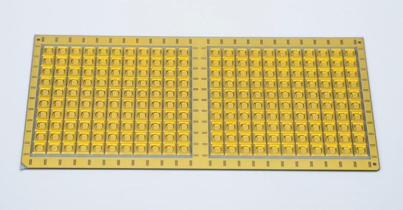
Choosing the right ceramic material defines your performance ceiling. You must match the material chemistry to your frequency requirements and operating temperatures.
An LTCC ceramic substrate is the optimal choice for high-frequency applications. Manufacturers fire LTCC materials at roughly 850°C to 900°C. This lower firing temperature yields a massive electrical advantage. It allows you to use highly conductive metals for internal routing. You can screen-print traces using gold, silver, or copper. These low-resistance metals minimize insertion loss at microwave and millimeter-wave frequencies. LTCC ensures your 5G and radar modules maintain pristine signal integrity.
HTCC requires firing temperatures above 1500°C. Silver and copper would melt entirely under these conditions. Therefore, HTCC requires refractory metals like tungsten and molybdenum. These metals have higher electrical resistance. This higher resistance makes HTCC less suitable for ultra-high-frequency RF signals.
However, HTCC offers exceptional structural rigidity. It provides higher thermal conductivity than LTCC. If your application involves extreme temperature environments, like deep-well drilling or engine control modules, HTCC delivers unmatched physical durability.
Additive manufacturing represents an emerging solution for ceramic packaging. 3D printing handles highly complex geometries that traditional tape-casting cannot achieve. You can print internal cooling channels or custom waveguide structures. Currently, 3D printed ceramics serve best for rapid prototyping. They help engineering teams validate physical layouts before committing to expensive hard tooling.
| Material Type | Metallization | Primary Advantage | Ideal Application |
|---|---|---|---|
| LTCC | Gold, Silver, Copper | Low signal loss, High-frequency support | RF, 5G, Radar, Telecom |
| HTCC | Tungsten, Molybdenum | Extreme physical durability, High thermal transfer | Aerospace, Downhole drilling, Automotive |
| 3D Printed | Variable | Complex geometries, Rapid turnarounds | Prototyping, Custom short runs |
You cannot blindly select a ceramic material. Engineering teams must evaluate specific physical and electrical metrics against their target outcomes.
Thermomechanical stress destroys solder joints. Bare silicon, SiC, and GaN dies expand as they heat up. If the substrate expands at a wildly different rate, the connection points shear. You must evaluate the substrate’s coefficient of thermal expansion (CTE). Ceramic materials naturally offer a CTE very close to bare semiconductors. By carefully matching the CTE, you minimize stress during severe power cycling. This alignment prevents microscopic fractures and ensures long-term field reliability.
Signal speeds demand precise dielectric controls. You must assess the Dielectric Constant (Dk) and Dissipation Factor (Df) based on your target frequency band.
Dielectric Constant (Dk): A stable Dk ensures predictable signal propagation speeds. It prevents phase shifts in phased-array radar systems.
Dissipation Factor (Df): A low Df minimizes the energy absorbed by the substrate. This keeps the signal amplitude strong over longer routing distances.
| Frequency Band | Target Dk Limit | Target Df Limit | Design Priority |
|---|---|---|---|
| Sub-6 GHz | < 9.0 | < 0.005 | Standard impedance control, stable power delivery. |
| 24 - 40 GHz | < 7.0 | < 0.002 | Minimize insertion loss, tight trace width tolerance. |
| 77 GHz+ (Radar) | < 5.0 | < 0.001 | Strict phase control, ultra-smooth conductor surfaces. |
Advanced ceramics carry higher non-recurring engineering (NRE) costs. Tooling, mask creation, and initial setup require significant upfront investment. You must define your production volume thresholds clearly. For small prototype runs, the initial expense appears high. However, as production scales, the cost per unit drops significantly. The performance gains—eliminated field failures and reduced warranty claims—quickly offset these initial expenses in high-reliability markets.
Transitioning to ceramic packaging introduces new manufacturing realities. Designers cannot treat a ceramic layout like a standard FR4 board.
You must perform advanced electro-thermal co-simulation before finalizing your design. Tools like Cadence or Ansys are essential. These platforms predict how heat flows through the dense multi-layer structure. They also model signal integrity across embedded passive components. Skipping this step is a common mistake. Without simulation, you risk creating internal thermal chokepoints or impedance mismatches that ruin the final product.
Ceramic materials shrink during the co-firing process. You can expect an X, Y, and Z-axis shrinkage of typically 10% to 15%. This physical reality complicates manufacturing. Vendors must manage tolerance controls meticulously to prevent layer misalignment. If internal vias shift during firing, open circuits occur. You must work closely with your fabrication partner. They use precise shrinkage control data to scale your original CAD files up before printing.
Custom ceramic tooling requires extended lead times. Standard FR4 fabrication might take days. Ceramic co-firing often takes several weeks for the initial run. Procurement teams must adjust project roadmaps accordingly. You must factor mask creation, test firing, and final inspection into your launch schedule. Rushing the process increases the risk of micro-cracking and yield drop-offs.
Engineering leaders need clear justification before switching material platforms. A structured approach ensures the transition yields measurable benefits.
Use a strict checklist to determine if a ceramic platform is necessary. Authorize the transition if your project hits any of the following triggers:
Continuous operating temperatures exceed 150°C.
System operating frequencies push past 30GHz.
Extreme miniaturization demands embedded passive components.
Deployment occurs in high-moisture or corrosive environments.
Bare die attachment requires strict CTE matching to prevent shear stress.
Not all fabrication facilities handle advanced ceramics well. You must vet your manufacturing partners strictly. Look for precise shrinkage control data from past runs. Verify they possess in-house metallization capabilities for gold and silver. Ensure they hold proper mil-spec testing certifications if you target defense sectors. A qualified vendor will gladly provide cross-section analysis reports proving their via alignment accuracy.
We recommend a phased rollout to mitigate risk. Do not jump straight to high-volume hard tooling.
Start with rigorous thermal and electrical EDA simulation.
Move to a 3D-printed ceramic prototype to prove the physical concept and mechanical fit.
Finalize the layout and transition to traditional LTCC or HTCC tooling for uniform volume production.
This phased approach protects your engineering budget and ensures design accuracy.
Upgrading your hardware architecture demands careful planning. While 3D ceramic substrates require higher upfront design rigor and initial investment, they are the only reliable path forward for next-generation electronics. They solve the critical thermal bottlenecks that plague standard organic materials. They provide the ultra-low parasitic environment necessary for emerging millimeter-wave technologies. By aligning your material selection with precise operational requirements, you guarantee long-term field reliability.
Now is the time to optimize your hardware roadmaps. We encourage technical directors and PCB designers to request a material spec sheet from a certified vendor. Submit your preliminary CAD files for a comprehensive manufacturability review. Consult directly with an application engineer to validate your internal thermal models. Taking these actionable steps today ensures your next product launch dominates in extreme environments.
A: The primary advantage is the lower firing temperature of LTCC. Because it fires around 850°C to 900°C, manufacturers can use highly conductive, low-resistance metals like silver, gold, and copper for internal routing. These metals drastically minimize insertion loss and preserve signal integrity at ultra-high RF and microwave frequencies.
A: No, not entirely. While 3D printing is excellent for fabricating complex geometries and supporting rapid new product introductions without expensive hard tooling, it scales poorly. Traditional tape-casting methods remain significantly more cost-effective, faster, and standardized for high-volume, uniform production runs.
A: MCPCBs rely on a thin dielectric layer between the circuit and the metal core. This dielectric layer inherently acts as a thermal bottleneck. 3D ceramics completely eliminate this insulating layer. They offer direct, highly efficient thermal pathways from the heat source to the sink, combined with perfectly matched thermal expansion rates.


