

Views: 0 Author: Site Editor Publish Time: 2026-07-04 Origin: Site


Modern microelectronics face unprecedented thermal and spatial constraints. Devices like wide-bandgap semiconductors, high-frequency RF modules, and advanced optoelectronics pack massive power into ever-shrinking physical footprints. Traditional 2D organic substrates, such as FR4 or polyimide, struggle to survive in these conditions. Standard metal lead frames also fail when exposed to extreme power densities and unpredictable operating environments. They simply cannot dissipate trapped heat fast enough to prevent catastrophic system failures.
We need a fundamental structural and functional paradigm shift to overcome these physical barriers. Enter the 3D Ceramic Packaging Substrate. This technology merges vertical integration techniques with superior material properties to solve crippling system-level bottlenecks. In the sections below, you will learn exactly how ceramic packaging outperforms organics. We will cover thermal management, miniaturization benefits, material options, and practical implementation frameworks.
Thermal & Structural Integrity: 3D ceramic substrates provide unmatched thermal conductivity and Coefficient of Thermal Expansion (CTE) matching with silicon/SiC dies, reducing mechanical stress.
Miniaturization: Enables true Z-axis integration (embedded passives, complex internal routing, cavity structures) to drastically reduce footprint.
RF & High-Frequency Stability: Low dielectric loss makes them optimal for 5G/6G, radar, and aerospace communications.
Implementation Reality: Upfront Non-Recurring Engineering (NRE) costs are higher, meaning adoption must be justified by strict performance, reliability, or miniaturization requirements.
Standard circuit board technologies dominate general electronics. They fall apart quickly at the bleeding edge of performance. Engineers constantly battle physical limits when designing next-generation hardware. You cannot force an organic board to behave like an advanced thermal conductor. Understanding these bottlenecks highlights exactly why advanced ceramics become necessary.
Materials like FR4 and standard plastics degrade rapidly under high operating temperatures. Organics possess terrible thermal conductivity properties. Heat gets trapped beneath high-power components. This forces engineering teams to bolt on bulky active cooling solutions. Heat sinks and fans consume valuable physical space. Prolonged exposure to temperatures above 130°C causes FR4 to warp, char, or delaminate completely. Your system reliability drops vertically as temperatures climb.
Radio frequency (RF) applications demand pristine signal integrity. Standard PCBs introduce severe parasitic losses at high frequencies. Dielectric inefficiencies ruin signal clarity in radar and satellite communications. The materials absorb the signal energy instead of transmitting it. High dielectric constants and unstable dissipation factors plague organic substrates. You cannot easily correct these parasitic losses through software or circuit tuning.
Traditional PCB design relies on spreading components across a flat two-dimensional plane. This surface-mounting approach wastes enormous amounts of space. When designing medical implants, aerospace payloads, or dense sensor arrays, horizontal real estate simply vanishes. You cannot miniaturize a device effectively if you only build outward. Rigid 2D boards severely limit your packaging density.
Non-hermetic packages leave sensitive components vulnerable. Standard plastic encapsulation absorbs moisture over long lifecycles. Chemical corrosion destroys microscopic wire bonds inside the package. Organics also suffer from outgassing in vacuum environments, like deep space. These outgassed polymers coat sensitive optical lenses or sensors nearby. Long-term deployment in harsh environments demands materials impervious to chemical and atmospheric intrusion.
Ceramics fundamentally alter how heat moves through a system. Materials like Alumina (Al2O3) and Aluminum Nitride (AlN) conduct heat exceptionally well. AlN can deliver thermal conductivity rates hundreds of times higher than typical FR4. It pulls heat rapidly away from high-power silicon carbide (SiC) or gallium nitride (GaN) dies.
Mechanical stress destroys more circuits than direct heat. The Coefficient of Thermal Expansion (CTE) measures how much a material grows when heated. Silicon dies expand slightly under load. Organic boards expand massively. This mismatch tears solder joints apart during aggressive thermal cycling. Ceramic CTE values align closely with silicon. They expand together and contract together. This synchronicity prevents solder joint fatigue and physical delamination.
True three-dimensional structures unlock massive space savings. You can stack dozens of ceramic layers vertically before the final firing process. These layers feature step cavities designed specifically for housing bare semiconductor dies. Engineers utilize blind and buried vias to connect signals vertically without consuming surface space.
Embedding passive components changes the entire footprint calculation. You can embed resistors, capacitors, and inductors directly into the inner ceramic layers. Moving these passives off the top surface shrinks the overall package significantly. The substrate transforms into an active participant in the circuit rather than just a dumb carrier board.
Millimeter-wave applications demand stable electrical environments. Ceramics boast incredibly low dielectric constants (Dk) and low dissipation factors (Df). They maintain signal integrity up to 100 GHz and beyond. The material does not absorb the radio energy passing through it.
Creating short, precisely controlled 3D interconnects reduces signal delay. Shorter routing paths naturally mitigate electromagnetic interference. Signals arrive faster and cleaner. 5G arrays and military radar modules rely heavily on these precise internal geometries to function correctly.
Dense, sintered ceramics offer a zero-porosity barrier against the outside world. Moisture, gases, and chemical contaminants cannot penetrate the solid ceramic walls. You achieve true hermeticity without needing heavy external metal enclosures.
This zero-porosity trait proves vital across several intense sectors. Deep-sea electronics survive crushing pressures and saltwater corrosion. Aerospace systems withstand extreme temperature swings and radiation. Sterile medical environments benefit because the ceramic withstands rigorous autoclave sterilization without degrading.
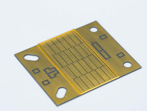
Choosing the right ceramic approach dictates your manufacturing success. Each category serves specific operational goals. We will break down the three primary manufacturing technologies dominating this space.
The HTCC substrate stands as the ultimate choice for extreme structural durability. It dominates high-power applications requiring absolute hermeticity. Manufacturers stack layers of ceramic tape and fire them simultaneously.
This process demands extreme firing temperatures exceeding 1500°C. Such intense heat limits your metallization options. You must use refractory metals like Tungsten or Molybdenum for internal routing. These metals survive the furnace but exhibit higher electrical resistance than copper or silver. Therefore, HTCC trades a slight bit of electrical efficiency for maximum physical and thermal robustness.
LTCC targets high-frequency RF, microwave, and complex mixed-signal modules. Researchers modified the ceramic powder chemistry by adding specific glass elements. This addition lowers the required firing temperature down to around 850°C to 900°C.
Lower firing temperatures unlock a massive advantage. You can use highly conductive metals like Silver, Gold, and Copper for internal traces. These metals offer superior electrical performance and low signal loss. LTCC delivers excellent RF stability but cannot quite match the raw thermal conductivity or structural rigidity of HTCC.
Additive manufacturing brings unprecedented geometric freedom to ceramics. It works best for rapid prototyping and generating highly complex geometries. You can print intricate internal cooling channels or severe overhangs. Traditional tape casting simply cannot produce these shapes.
However, reality checks remain necessary. Current 3D printing methods face severe limitations regarding mass-production scalability. Integrating multiple metal routing layers during the printing process remains difficult. Furthermore, managing dimensional shrinkage tolerances requires intense calibration. Co-firing traditional tape layers currently offers more predictable high-volume yields.
| Technology Type | Ideal Application | Typical Firing Temp | Supported Metals | Key Trade-off |
|---|---|---|---|---|
| HTCC | High-power, extreme harsh environments | > 1500°C | Tungsten, Molybdenum | Higher electrical resistance in traces |
| LTCC | High-frequency RF, mixed-signal arrays | 850°C - 900°C | Silver, Gold, Copper | Lower thermal conductivity vs HTCC |
| 3D Printed | Prototyping, complex internal channels | Varies by binder | Challenging co-integration | Low volume scalability, tight tolerances |
Transitioning away from organic boards requires deliberate financial and engineering adjustments. You must evaluate these realities before committing to a ceramic design. Failing to understand the manufacturing differences leads to blown budgets and delayed launches.
Expect high upfront Non-Recurring Engineering (NRE) costs. Manufacturers build custom punch tools to create thousands of tiny vias in the ceramic tape. They fabricate precise metal stencils for screen-printing the conductive pastes. Establishing custom firing profiles for the furnace also takes engineering hours. These initial setup steps require significant capital before the first board ever ships.
Ceramic layers shrink significantly during the final sintering process. Shrinkage rates typically range between 15% and 20% along the X and Y axes. Engineering teams must scale their initial CAD drawings perfectly to account for this reduction.
Common Mistake: Applying FR4 design rules to ceramic layouts.
Best Practice: Engage your fabrication partner during the earliest schematic phase to verify shrinkage calculations.
Tight tolerances remain critical to ensure pad alignment across multiple stacked layers. A slight miscalculation causes buried vias to miss their targets entirely, ruining the batch.
High-end 3D ceramic manufacturing relies on highly specialized fabrication partners. You cannot order these substrates from generic overseas rapid-prototyping shops. Securing slots in industrial high-temperature furnaces takes time. Consequently, expect potentially increased lead times compared to standard rigid PCBs. You must build these lead times into your product development schedule.
Evaluators often suffer sticker shock when comparing bare component costs. A single ceramic package easily outprices a comparable FR4 board. However, you must use a broader evaluation lens.
Using ceramics eliminates the need for expensive active cooling fans. It removes heavy secondary metal housings. It absorbs dozens of distinct passive components into the substrate itself. Eliminating these external factors often results in a significantly lower total system cost. You gain reliability and shrink the device size while balancing the overall financial expenditure.
Deciding when to abandon organics requires a systematic approach. You should not default to ceramics for simple consumer gadgets. Use this framework to determine if the technology fits your specific engineering challenges.
Define absolute trigger points for your project. The shift to ceramics becomes mandatory when your design hits specific physical walls.
Thermal Threshold: Operating temperatures consistently exceed 150°C.
Frequency Threshold: Signal frequencies push beyond the 30GHz millimeter-wave boundary.
Environmental Threshold: Mandated true hermeticity against moisture or chemical exposure.
If your project triggers any of these three conditions, organic boards pose a severe risk to product viability.
You must weigh your intended production volume against available technologies. Additive 3D printed ceramics win heavily in the prototyping phase. They require zero tooling costs for quick iterations. However, as you scale into high-volume production, HTCC and LTCC technologies scale much better. The high initial NRE costs amortize rapidly across large production runs. Map out your projected three-year volume before selecting a primary manufacturing method.
Engineering teams should follow specific steps once they shortlist ceramics. First, execute detailed thermal simulation modeling. Prove that the heat dissipation matches your mathematical expectations. Second, consult directly with substrate fabrication engineers early in the schematic phase. Do not finalize routing without their input on shrinkage tolerances. Third, request standard material test data. Verify the specific dielectric and thermal properties of their proprietary ceramic blends.
We must recognize that 3D ceramic packaging substrates are not generic PCB replacements. They represent highly specialized architectural choices engineered for overcoming critical thermal, spatial, and environmental barriers. By matching CTE with silicon dies, delivering true hermeticity, and unlocking vertical integration, ceramics solve problems organics cannot touch.
Adopting this technology requires a thorough understanding of firing processes, shrinkage constraints, and initial tooling costs. However, eliminating bulky cooling systems and external housings justifies the investment. Evaluate your performance thresholds carefully. Schedule a technical consultation with a fabrication expert, download comprehensive material specification design guides, or submit your early CAD files for a rigorous DFM review today.
A: The upfront component cost of a ceramic substrate is notably higher due to specialized tooling and complex firing processes. However, ceramics often eliminate the need for secondary housings, active cooling mechanisms, and separate passive components. This integration frequently leads to overall system-level financial savings and drastically improved lifecycle reliability.
A: HTCC refers to a specific manufacturing process (High-Temperature Co-fired Ceramic), whereas AlN refers to a raw material. You can process AlN powder using HTCC methods. Combining the AlN material with the HTCC process yields a substrate offering absolute maximum thermal conductivity and structural hermeticity.
A: Yes, you can easily integrate standard SMT components. Ceramic substrates fully support traditional SMT soldering techniques. They also offer broad compatibility with advanced attachment methods, including standard wire bonding and direct flip-chip mounting, providing immense flexibility for mixed-technology assemblies.
A: Lead times generally run longer than standard PCBs. Creating custom punch tools, calibrating tape casting machines, and executing precise co-firing cycles require specialized engineering. You should set realistic expectations and typically plan for multiple weeks of engineering and tooling before initial physical prototypes arrive.


