

Views: 286 Author: Site Editor Publish Time: 2026-07-03 Origin: Site


As power densities in modern electronics surge, traditional organic substrates hit hard thermal and spatial limits. Systems driving electric vehicles, advanced 5G/6G RF arrays, and aerospace modules demand far more than standard FR4 boards. Even flat 2D ceramics increasingly struggle to accommodate modern spatial constraints. Engineers now transition toward true 3D architectures to solve these pressing bottlenecks. This architectural shift enables seamless heterogeneous integration while maximizing vertical space utilization. You can embed passives and stack components vertically to achieve unprecedented design density. Consequently, the 3D Ceramic Packaging Substrate emerges as the critical enabler for highly reliable, next-generation electronic modules. It balances extreme thermal demands and aggressive miniaturization requirements seamlessly. We will explore how these advanced structures resolve chronic heat issues, detail the core evaluation criteria for selection, and navigate the complex manufacturing realities governing their adoption today.
Thermal Supremacy: 3D ceramic substrates provide unmatched heat dissipation for high-density components, preventing thermal throttling in advanced ICs and power modules.
CTE Compatibility: Precision Coefficient of Thermal Expansion (CTE) matching with Silicon (Si) and Silicon Carbide (SiC) drastically reduces mechanical stress and solder joint fatigue.
Design Density: Vertical (3D) integration allows for shorter signal paths, reducing parasitic losses in high-frequency RF and microwave applications.
Manufacturing Shift: Evaluating these substrates requires balancing the high performance of materials (AlN, Al2O3) against the complexities of modern manufacturing (LTCC/HTCC vs. emerging ceramic 3D printing).
Flat ceramic boards served the electronics industry well for decades. However, they are no longer sufficient for complex System-in-Package (SiP) and multi-chip modules (MCM). Modern designs cluster high-power logic, memory, and power delivery networks into incredibly tight spaces. When you place these components on a flat 2D plane, the horizontal footprint expands drastically. This horizontal sprawl defeats the primary goal of miniaturization. Furthermore, lateral heat spreading on a 2D surface often proves inadequate. Heat gets trapped between closely packed bare dies. You inevitably encounter localized hotspots. These hotspots degrade semiconductor performance and accelerate device failure.
Moving into the Z-axis becomes an absolute imperative. 3D architectures completely redefine spatial management. They allow you to utilize embedded passive components directly inside the substrate. You can route complex signals through internal vias. You can also design stepped cavity structures. These stepped cavities house bare dies securely. They protect sensitive silicon components while drastically saving horizontal space. By stacking logic and power devices vertically, you consolidate the entire module volume. This approach proves invaluable for spatial-constrained environments like aerospace modules and implantable medical devices.
Signal integrity represents another massive hurdle for traditional layouts. Longer organic substrate wire bonds introduce significant parasitic inductance. High-frequency signals degrade rapidly over these extended physical distances. This degradation causes unacceptable data loss in high-speed 5G and radar applications. Vertical 3D ceramic routing directly mitigates this issue. It creates the shortest possible path between stacked chips. Shorter paths reduce parasitic capacitance. They ensure pristine signal integrity even at millimeter-wave frequencies. We see immediate performance gains when converting legacy 2D layouts into optimized 3D structures.
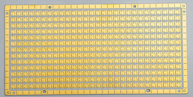
Specifying a high power ceramic substrate requires strict adherence to demanding performance baselines. Thermal conductivity stands as the primary evaluation metric. Power electronics generate immense localized heat. Standard FR4 boards simply melt or delaminate under such thermal stress. Engineers typically evaluate two primary ceramic materials. Aluminum Oxide (Al2O3) provides a baseline performance of roughly 20-30 W/m·K. It handles moderate power applications effectively. Conversely, Aluminum Nitride (AlN) delivers extreme performance. It boasts thermal conductivity ranging from 170 to 230 W/m·K. You must select AlN for silicon carbide (SiC) and gallium nitride (GaN) power modules.
| Material Property | Aluminum Oxide (Al2O3) | Aluminum Nitride (AlN) | Standard FR4 (For Reference) |
|---|---|---|---|
| Thermal Conductivity (W/m·K) | 20 - 30 | 170 - 230 | 0.2 - 0.3 |
| Coefficient of Thermal Expansion (ppm/K) | 6.5 - 7.5 | 4.0 - 4.5 | 14 - 17 |
| Dielectric Constant (Dk at 1MHz) | 9.0 - 10.0 | 8.5 - 9.0 | 4.2 - 4.8 |
| Primary Application Focus | General microelectronics | High-power and RF modules | Low-power consumer devices |
Dielectric performance dictates success in high-frequency applications. Dense 3D structures pack signal traces closely together. This proximity invites severe cross-talk and signal delay. You must evaluate the dielectric constant (Dk) and loss tangent (Df) of your chosen material. A lower loss tangent minimizes energy dissipation into the substrate. This efficiency ensures maximum signal transmission power. High-purity ceramics offer highly stable dielectric properties across vast temperature ranges. This stability is critical for radar arrays and satellite communications.
Thermomechanical reliability directly determines device lifespan. Devices undergo thousands of power cycles. They heat up and cool down rapidly. Silicon dies have a Coefficient of Thermal Expansion (CTE) of roughly 3 ppm/K. Standard organic boards have a CTE of 15 ppm/K or higher. This massive mismatch tears solder joints apart during thermal cycling. Warping and cracking inevitably follow. A high-performance ceramic perfectly bridges this gap. AlN features a CTE of roughly 4.5 ppm/K. This close match virtually eliminates mechanical stress on delicate solder bumps.
Hermeticity represents the final critical baseline. Aerospace controls, automotive sensors, and medical implants operate in unforgiving environments. They require absolute barriers against moisture and corrosive gases. Traditional polymers absorb moisture over time. Ceramics achieve true zero-porosity. A properly fired ceramic substrate creates an impenetrable hermetic seal. This structural density prevents oxidation of internal copper or gold routing. We always mandate hermetic testing for mission-critical deployments.
You must understand the distinct manufacturing methods to deploy these substrates successfully. The industry relies heavily on High-Temperature Co-fired Ceramics (HTCC) and Low-Temperature Co-fired Ceramics (LTCC). Each process carries specific constraints and advantages.
HTCC processes require firing temperatures exceeding 1400°C. This extreme heat mandates the use of refractory metals like tungsten or molybdenum for internal routing. These metals offer robust structural integrity. However, they exhibit higher electrical resistance than copper or gold. HTCC excels in extreme high-power scenarios. LTCC operates differently. It fires below 900°C. This lower temperature allows engineers to use highly conductive silver or gold pastes. LTCC dominates high-frequency RF applications due to superior electrical conductivity. Both traditional methods share common drawbacks. They require expensive tooling setups. They suffer from long lead times. They also impose strict design limitations regarding complex internal cavities.
Additive manufacturing disrupts these traditional paradigms completely. Ceramic 3D printing is rapidly transforming prototyping and low-volume production phases. Engineers can now print complex stepped cavities and intricate cooling channels directly. We bypass expensive tooling stages entirely. You can iterate designs in days rather than months. This agility accelerates development cycles for cutting-edge modules.
Despite these advantages, you must adopt a skeptical, evidence-based view on 3D printed ceramics. We face distinct adoption risks. Additive manufacturing eliminates tooling, but it introduces structural variables. You must rigorously verify printing yield rates. Surface finish tolerances often require post-processing to meet tight semiconductor mounting standards. Furthermore, the structural density of printed ceramics sometimes lags behind pressed and fired equivalents. You must test structural integrity meticulously before full-scale deployment.
| Process Type | Conductive Metals Used | Lead Time | Geometric Freedom |
|---|---|---|---|
| HTCC | Tungsten, Molybdenum | High | Low to Medium |
| LTCC | Gold, Silver, Copper | High | Medium |
| 3D Printing | Silver nanoparticles (typical) | Low | Exceptionally High |
Evaluating substrates demands a shift from component-level specifications to comprehensive system-level performance. Advanced packaging fundamentally alters module architecture. A high-performance substrate natively handles massive thermal loads. This inherent capability often eliminates the need for bulky secondary cooling systems. You can strip away heavy aluminum heatsinks. You can remove mechanical cooling fans. By eliminating these secondary components, you achieve a significantly lighter, more compact final product. System reliability improves drastically when you remove moving parts like fans.
Procurement teams must apply rigorous shortlisting logic when selecting substrate partners. You cannot evaluate these vendors the same way you evaluate standard PCB suppliers. The manufacturing complexity requires specialized expertise. We recommend utilizing a structured vendor evaluation checklist. Focus heavily on documented quality control and internal testing capabilities.
Demonstrated Yield Rates: Request verified yield data for multi-layer 3D structures. High layer counts drastically increase the difficulty of precise via alignment.
In-House Testing Validation: Ensure the vendor performs rigorous in-house thermal cycling. They must validate hermetic sealing through helium leak testing.
Agile Lead Times: Map out the exact lead times for design iterations. Clarify their capabilities regarding tooling approaches versus additive manufacturing methods.
Regulatory Compliance: Demand proof of compliance with strict industry standards. Look for MIL-PRF-38534 certification for defense applications. Require AEC-Q200 compliance for automotive deployments.
We advise implementing specific next-step actions before committing to full production. Start your journey with advanced thermal simulation. Utilize Electronic Design Automation (EDA) tools to model your heat distribution accurately. Identify precise hotspots before ordering physical parts. Next, order additive-manufactured prototypes. Validate your electrical and thermal models using these printed samples. Prove your design concept thoroughly. Once validated, you can confidently transition to high-volume LTCC or HTCC tooling. This phased approach mitigates structural risks and accelerates final deployment.
Acknowledge the Niche: 3D ceramic packaging is not a universal replacement for standard organic PCBs. It serves as a mandatory upgrade specifically for high-power, high-frequency, and harsh-environment applications.
Collaborate Early: Successful adoption relies on immediate collaboration. PCB designers, thermal engineers, and substrate manufacturers must align their goals during the initial drafting phase.
Audit Your Failures: Analyze your current field returns. Audit your existing thermal failure rates to identify where ceramic structures can resolve chronic overheating.
Test Iteratively: Consult specialized substrate vendors for prototype feasibility. Leverage additive manufacturing to validate complex internal cavity designs rapidly.
Prioritize Material Matching: Always align your substrate's CTE with your dominant semiconductor material to ensure maximum lifespan.
A: A standard PCB uses organic FR4 material across 2D layers. FR4 offers poor heat transfer and limits integration depth. Conversely, an inorganic ceramic substrate provides excellent heat transfer. It allows for customized 3D cavities, internal vertical routing, and true hermetic sealing. Ceramics withstand extreme temperatures that would instantly destroy organic boards.
A: MCPCBs handle bulk heat efficiently. However, they struggle with electrical isolation and signal integrity. You specify ceramics when you need superior dielectric strength and high-frequency RF performance. Ceramics completely eliminate the severe parasitic capacitance issues inherently found in metal-backed boards.
A: They are highly viable for rapid prototyping, complex geometric designs, and specialized low-to-medium volume runs. The technology accelerates development immensely. However, traditional LTCC and HTCC methods often remain more reliable and efficient for scaling into millions of standardized units. Engineers must balance volume needs against geometric complexity.


