

Views: 0 Author: Site Editor Publish Time: 2026-07-02 Origin: Site


Evaluating the production process of advanced IC packaging helps you determine technical feasibility, scalability, and vendor capabilities. You need to know exactly how components are built. This knowledge ensures your supply chain remains robust and reliable. The manufacturing method directly impacts thermal performance, high-frequency signal integrity, production lead times, and unit economics. Without understanding the underlying production mechanics, you risk encountering severe schedule delays or compromised product reliability. Navigating the current shift from traditional subtractive and laminated methods, like HTCC and LTCC, to emerging additive manufacturing requires careful attention. You must align material science innovations alongside commercial production realities to succeed. In this article, you will learn the exact steps involved in substrate manufacturing. We will compare traditional co-firing against modern 3D printing techniques. You will also discover actionable frameworks for mitigating yield risks. Finally, we provide strategies to help you select the right manufacturing partner for your specific electronic packaging requirements.
Process Dictates Performance: Traditional multi-layer co-firing (LTCC/HTCC) provides unmatched hermeticity, while additive 3D printing accelerates prototyping and enables complex internal geometries.
Material Alignment: Selecting an alumina ceramic substrate provides a baseline for cost-to-performance, but high-power applications may require AlN (Aluminum Nitride) or specialized LTCC tapes.
Yield Risks: The most critical evaluation points for manufacturing partners are shrinkage tolerance control during co-firing and precise via-alignment in high-layer-count stacks.
Vendor Selection: Shortlisting should rely on verified capabilities in minimum line width/spacing, layer limits, and compliance with military or aerospace testing standards.
Understanding different manufacturing approaches is crucial for planning your product lifecycle. Engineers must evaluate production methods based on volume requirements and design complexity. The industry primarily categorizes these methods into traditional co-firing and emerging additive manufacturing. Each approach offers distinct mechanical advantages and specific production constraints.
Traditional co-firing relies on a well-documented sequence of subtractive and laminated processes. The core mechanism includes tape casting, mechanical punching, screen printing, and layer lamination. Operators process raw ceramic materials into thin, flexible sheets before firing them. This method remains the backbone of the electronic packaging industry.
These traditional methods are best for scalable, high-volume production. They deliver proven hermeticity and provide established reliability data. Decades of industry testing back HTCC and LTCC performance metrics. You can trust these methods for critical aerospace or medical applications. The processes guarantee tight environmental seals and long-term durability.
However, traditional methods carry specific limitations. They require high upfront tooling costs to create custom punches and screens. Design iterations suffer from longer lead times. You must follow strict design rule limitations regarding internal cavities and complex routing. Making sudden design changes mid-production is highly inefficient and resource-intensive.
Additive manufacturing introduces entirely new design possibilities. The primary mechanisms include stereolithography (SLA) or direct ink writing. Printers use specialized ceramic slurries to build parts layer by layer. After printing, technicians subject the green parts to debinding and sintering. This process solidifies the ceramic matrix.
Ceramic 3D printing is best for rapid prototyping. It enables complex 3D internal cooling channels previously impossible to machine. You can execute low-volume, high-mix production runs efficiently. Engineers can test multiple iterations in weeks rather than months. It fundamentally accelerates new product introduction cycles.
Despite these benefits, additive manufacturing faces notable limitations. Volume scalability constraints remain a significant hurdle. Printers cannot match the sheer output speed of traditional tape casting lines. You may encounter variations in surface roughness across different build orientations. Furthermore, the industry is still maturing metallization techniques for printed parts. Integrating conductive traces directly into printed structures remains challenging.
| Feature | Traditional Co-Firing (HTCC/LTCC) | Additive Manufacturing (3D Printing) |
|---|---|---|
| Core Mechanism | Tape casting, punching, and lamination | SLA or direct ink writing layer-by-layer |
| Volume Capability | Excellent for high-volume production | Best for low-volume, high-mix runs |
| Design Flexibility | Strict limits on internal cavities | Unmatched freedom for complex geometries |
| Tooling Investment | High upfront tooling required | Minimal tooling required |
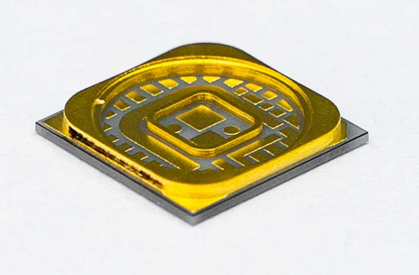
Creating a reliable package requires extreme precision across multiple steps. Every phase influences the final structural and electrical integrity. You must understand where process control directly impacts final product quality. Minor deviations early in the process compound into catastrophic failures during final testing.
Slurry Preparation & Tape Casting: Production begins by mixing raw ceramic powder with specific organic binders and solvents. This mixture forms a homogeneous slurry. Machines cast this slurry onto a carrier film to create thin, flexible sheets called green tapes. Buyer consideration: The vendor's control over tape thickness consistency is vital. Uneven thickness dictates varied final electrical characteristics and impedance mismatches.
Via Punching & Filling: Technicians create microscopic holes through the green tape. These holes serve as vertical interconnects between different layers. Manufacturers use mechanical punches or lasers for this step. Next, they fill these vias with specialized conductive pastes. Buyer consideration: Assess mechanical versus laser punching limits. Laser punching generally achieves a smaller minimum via diameter. This allows for higher density routing.
Metallization & Circuit Printing: Operators apply conductive pastes to the tape surface using fine mesh screens. This step prints the horizontal circuitry. HTCC requires refractory metals like tungsten or molybdenum to withstand extreme firing heat. LTCC uses highly conductive metals like silver, gold, or copper. Proper paste rheology ensures crisp, defined trace edges.
Stacking, Lamination, & Co-Firing: The printed layers are carefully stacked and optically aligned. A specialized press compresses the stack under precise heat and pressure. Finally, the laminated stack enters a high-temperature furnace for sintering. The organic binders burn away, and the ceramic particles fuse. Buyer consideration: Shrinkage during sintering typically ranges from 12 to 15 percent. This requires exact predictive modeling by the manufacturer. They must maintain strict dimensional tolerances to ensure component fitment.
Common Mistakes: Overlooking the debinding profile often leads to trapped carbon residues. These residues cause internal delamination. You should verify your partner uses controlled atmospheric conditions during the entire sintering cycle.
Your material selection dictates the operational limits of your final device. Engineers must balance thermal conductivity, mechanical strength, and electrical properties. Let us examine the three primary material families used in electronic packaging today.
Alumina (Al₂O₃) Ceramic Substrate:
This material represents the industry standard for baseline HTCC and thick-film applications. Selecting an alumina ceramic substrate provides a proven balance of mechanical strength and cost-efficiency. It offers acceptable thermal conductivity for most standard microelectronics. You can rely on alumina for excellent chemical resistance. It performs exceptionally well under harsh environmental conditions.
Aluminum Nitride (AlN):
Engineers choose AlN when thermal management becomes the primary bottleneck. It dissipates heat rapidly, making it ideal for high-power LEDs and advanced power modules. AlN boasts a coefficient of thermal expansion closely matching silicon. This matching prevents stress fractures during extreme temperature cycling. However, you will face higher raw material and processing costs compared to alumina.
Glass-Ceramic Composites (LTCC Materials):
These composite materials incorporate glass elements to lower the required firing temperatures significantly. The lower heat allows for highly conductive traces, such as pure gold, silver, or copper. You minimize resistive losses drastically. This material is ideal for high-frequency RF and microwave applications. It requires low dielectric loss to maintain signal integrity at high gigahertz bands.
Best Practices: Always match the substrate material's thermal expansion coefficient to your primary semiconductor die. A severe mismatch causes solder joint fatigue over time. You must run thermomechanical simulations early in the design phase.
Securing a well-manufactured 3D Ceramic Packaging Substrate demands rigorous validation. You cannot assume high yield rates without auditing the facility's quality control protocols. Let us break down the most critical risks and the standards required to mitigate them.
Ceramics shrink dramatically during the transition from a green state to a fired solid. You must know how the manufacturer models and controls X, Y, and Z-axis shrinkage. Shrinkage occurs during both the debinding and sintering phases. Uneven shrinkage leads to severe substrate warpage. Warped substrates prevent successful automated surface mount assembly down the line.
Multi-layer packages demand flawless optical alignment. Precision is non-negotiable. The impact of layer misalignment is severe. Minor deviations in 20-plus layer stacks lead to parasitic capacitance. In worst-case scenarios, misalignment causes dead shorts between power and ground planes. You should ask vendors about their layer-to-layer registration tolerances.
Protecting delicate semiconductor dies requires a perfect environmental seal. Microscopic voids compromise the package's hermeticity. Moisture ingress quickly degrades internal wire bonds. Manufacturers use strict testing protocols to ensure integrity. Helium leak testing detects incredibly small fissures. Acoustic microscopy visualizes internal voids without destroying the part. You must demand these tests for mission-critical components.
Robust traceability ensures accountability across the supply chain. You need documentation tracking every raw material batch. Strict requirements exist for various industries. Evaluate requirements for ISO 9001 baseline quality. Look for IATF 16949 if you operate in the automotive sector. Demand MIL-PRF-38534 certifications for military and aerospace applications. These standards guarantee repeatable process controls.
| Defect Type | Testing Protocol | Primary Mitigation Strategy |
|---|---|---|
| Internal Delamination | Scanning Acoustic Microscopy (SAM) | Strict temperature profiling during debinding |
| Seal Failure | Helium Fine Leak Testing | Optimized paste-to-tape adhesion parameters |
| Electrical Shorts | Automated Optical Inspection (AOI) | High-precision optical alignment machines |
| Dimensional Warpage | Laser Profilometry | Advanced shrinkage predictive modeling software |
Selecting the right production partner defines your project's ultimate success. You must look beyond simple capability lists. A systematic framework helps you evaluate vendors objectively. Assess their technical depth, transparency, and ability to scale alongside your product roadmap.
Start by evaluating the vendor's production flexibility. Does the vendor offer ceramic 3D printing for early-stage New Product Introduction (NPI)? Fast iterations during NPI save crucial development months. Ask how smoothly they transition prototype designs into traditional LTCC or HTCC for volume manufacturing. A seamless internal handoff prevents costly redesigns.
You must scrutinize their published manufacturing limits. Evaluate their technical minimums on line width and spacing. Can they reliably print 50µm lines, or are they limited to 100µm? Check their minimum via diameters and maximum layer counts. Vendors pushing the boundaries of layer counts demonstrate superior alignment technology. Ensure their limits exceed your most complex design requirements.
Determine the full scope of their operational capabilities. Assess if the vendor solely provides the bare substrate. Many advanced foundries offer complete turnkey assembly. They perform internal wire bonding, flip-chip die attachment, and final lid sealing. Integrated services reduce shipping delays between multiple subcontractors. This consolidation drastically lowers the risk of handling damage.
Trust requires complete data transparency. Require prospective vendors to share historical yield rates for designs similar to your requirements. They should have robust Design for Manufacturing (DFM) feedback processes. A strong partner reviews your initial CAD files and suggests geometry tweaks. They highlight areas prone to shrinkage stress before cutting any tools.
Common Mistakes: Selecting a vendor based solely on theoretical capability charts often leads to disappointment. Always request a physical audit or review specific case studies matching your complexity level.
The successful manufacturing of advanced packaging substrates demands strict process mastery. Whether utilizing traditional co-firing or modern additive methods, engineers face the same fundamental challenges. You must actively manage material shrinkage, thermal dynamics, and alignment tolerances to achieve high yields. These factors define the physical limits of your microelectronic systems.
Choosing the correct foundational material heavily dictates your process route. Selecting an industry-standard alumina setup provides cost-efficiency and reliability. Alternatively, choosing an AlN variant solves extreme thermal bottlenecks but requires specialized handling. You must weigh these material decisions against your intended manufacturing method early in the product lifecycle.
Take immediate action to secure your supply chain. We highly recommend engaging with qualified manufacturers during the early CAD and Gerber design stages. Run comprehensive DFM checks to catch routing errors. Always validate prototype lead times and material availability before committing to a high-volume production foundry.
A: Lead times depend heavily on the chosen manufacturing method. Traditional HTCC/LTCC processes require hard tooling, pushing initial lead times to 6-10 weeks. Additive manufacturing via 3D printing bypasses tooling entirely. This drops prototyping lead times down to 1-3 weeks. Volume production runs require specific scheduling agreements.
A: Yes, it is rapidly approaching parity. Traditional co-firing currently offers the highest density and most consistent pore structures. However, advanced 3D printed ceramics achieve near-theoretical density after proper sintering. While suitable for many commercial uses, 3D printed parts still require rigorous lot-by-lot validation for strict aerospace or mil-spec standards.
A: Alumina substrates provide superior thermal conductivity and unmatched reliability in harsh environments. Crucially, they offer a Coefficient of Thermal Expansion (CTE) that closely matches silicon dies. This alignment prevents mechanical stress and solder joint fatigue during rapid temperature cycling. Organic PCBs simply cannot survive these extreme operational demands.
A: Shrinkage is managed using specific scaling factors integrated directly into the CAD layout. The manufacturing foundry provides these exact multipliers. They calculate the factors based on their unique slurry compositions and proprietary firing profiles. Designers enlarge the green state CAD model to ensure the final sintered part meets precise dimensional tolerances.


