

Views: 0 Author: Site Editor Publish Time: 2026-07-01 Origin: Site


For advanced electronics facing extreme thermal loads, physical space constraints, or high-frequency demands, standard organic packaging often becomes the failure point. Traditional 2D solutions simply cannot handle modern thermal densities. The shift toward a 3D Ceramic Packaging Substrate is rarely driven by initial budget considerations; it is driven by pure engineering necessity. Whether utilizing LTCC multi-layering or emerging additive manufacturing, engineers must justify this transition based on strict reliability criteria. Standard FR4 boards burn out or leak under such immense stress.
This guide breaks down the core commercial applications, material evaluation frameworks, and implementation risks. We will help your engineering team decide if this specialized architecture is the correct path for your next IC or MEMS project. You will discover exactly how to balance thermal management requirements against complex manufacturing realities.
Primary Use Cases: Essential for RF/microwave communications, aerospace defense systems, implantable medical devices, and high-power optoelectronics.
Core Advantage: Combines vertical spatial integration (3D routing) with the unmatched thermal conductivity and hermeticity of a ceramic substrate.
Evaluation Criteria: Vendor selection hinges on material properties (AlN vs. Alumina), manufacturing approach (LTCC vs. HTCC vs. Additive), and specific Coefficient of Thermal Expansion (CTE) matching capabilities.
Adoption Risk: Upfront tooling costs and longer prototyping lead times require rigorous pre-validation before volume scaling.
Dense 3D IC stacking creates severe heat traps. Standard FR4 or organic substrates cannot dissipate this trapped thermal energy effectively. When chips operate continuously at peak loads, they generate localized hotspots. These hotspots cause rapid degradation of internal circuitry. A ceramic substrate provides a highly efficient, thermally conductive escape path. It channels heat away from sensitive silicon dies, reducing device failure rates significantly. You must prioritize thermal escape routes when designing multi-chip modules.
Engineers face a constant battle between miniaturization and reliability. The market demands smaller physical footprints every year. However, we cannot sacrifice hermeticity to achieve these smaller sizes. Moisture and gas sealing remain absolute requirements for long-term operational stability. Organic materials absorb moisture over time, leading to internal corrosion. Ceramic materials offer near-zero moisture absorption. They form an impenetrable barrier around sensitive components.
High-frequency signal integrity presents another major hurdle. At 5G, 6G, and automotive radar frequencies, dielectric loss must be minimized. High-frequency signals degrade quickly when traveling through inferior dielectric materials.
Shorter Signal Paths: Vertical 3D routing reduces the physical distance signals must travel between components.
Impedance Control: Highly stable dielectric properties allow for exact impedance matching across multiple layers.
Crosstalk Reduction: Embedded shielding within the ceramic layers prevents signal interference between closely stacked communication channels.
Radar modules and satellite communication components operate in brutal conditions. They must survive extreme temperature cycling in low-earth orbit. Radiation resistance is non-negotiable for space-bound hardware. Strict hermetic sealing compliance ensures internal gases do not leak into a vacuum. Components typically undergo rigorous validation to meet these demands.
Standard testing protocols for these environments often include:
Fine leak testing using helium mass spectrometry to detect micro-fractures.
Gross leak testing via fluorocarbon bubbling to identify major seal failures.
Thermal shock cycling between extreme temperature ranges according to MIL-STD-883.
Modern autonomous vehicles rely heavily on LiDAR arrays and 77GHz automotive radar sensors. Base station transceivers also process massive amounts of high-frequency data. These applications require a low dielectric constant. A low loss tangent ensures signal fidelity remains high throughout complex 3D routing. If the substrate absorbs too much signal energy, the radar loses its detection range. Ceramic materials maintain consistent electrical properties across wide temperature fluctuations.
Pacemakers, neural implants, and micro-sensors demand flawless execution. Absolute biocompatibility is a baseline requirement for anything placed inside the human body. Extreme miniaturization allows for less invasive surgical procedures and greater patient comfort. Zero-leakage hermeticity is critical here. It protects the internal circuitry from corrosive bodily fluids over decades of use. Even a microscopic breach would lead to catastrophic device failure.
Laser diodes and dense LED arrays generate intense, localized thermal energy. They require rapid heat dissipation to maintain wavelength stability. If a laser diode overheats, its emission wavelength shifts. This ruins optical communication links or precise cutting tools. Rapid thermal management also prolongs the overall operational lifespan of the diode. Advanced ceramic packaging moves this heat outward instantly.
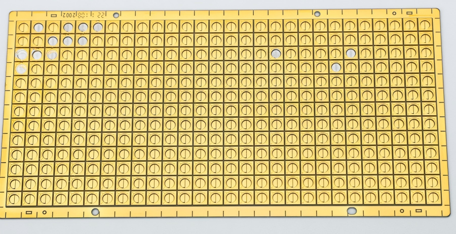
Choosing between Low-Temperature Co-fired Ceramic (LTCC) and High-Temperature Co-fired Ceramic (HTCC) dictates your electrical performance ceiling. LTCC fires at lower temperatures. This allows manufacturers to use highly conductive metals like gold, silver, and copper for internal routing. It is significantly better for high-frequency applications. HTCC requires high-temperature firing. This necessitates the use of refractory metals like tungsten or molybdenum. These metals have higher electrical resistance, causing more signal loss at high frequencies. However, HTCC provides superior structural strength and thermal conductivity.
Chart: LTCC vs. HTCC Core Differences
| Feature | LTCC (Low-Temperature) | HTCC (High-Temperature) |
|---|---|---|
| Firing Temperature | ~850°C to 900°C | ~1500°C to 1600°C |
| Trace Metals | Gold, Silver, Copper | Tungsten, Molybdenum |
| Electrical Conductivity | Excellent (Low resistance) | Moderate (Higher resistance) |
| High-Frequency Suitability | Optimal | Sub-optimal due to signal loss |
| Mechanical Strength | Good | Superior |
The base ceramic powder you select changes everything about thermal management. Alumina is the prevailing industry standard. It remains highly cost-effective while delivering excellent mechanical strength. It works perfectly for moderately demanding applications. Aluminum Nitride (AlN) is chosen when extreme thermal conductivity becomes the critical success factor. It pulls heat away from dense silicon dramatically faster than Alumina. Crucially, AlN often matches the CTE of silicon chips perfectly, preventing stress fractures.
| Material System | Thermal Conductivity (W/m·K) | Primary Use Case |
|---|---|---|
| Alumina | 20 - 30 | Standard robust electronics, general RF modules |
| Aluminum Nitride (AlN) | 170 - 230 | High-power lasers, dense CPU/GPU packaging |
Traditional manufacturing relies on tape-casting, screen printing, and sintering. This process scales beautifully. It is best for proven, high-volume production runs where designs are locked. However, it requires expensive physical tooling. Emerging ceramic 3D printing offers a radical alternative. Additive manufacturing is ideal for rapid prototyping. It allows teams to create internal cooling channels and complex geometries impossible with traditional tooling. You can iterate designs in days rather than months.
The transition to 3D ceramics involves significant hurdles. You must acknowledge the high initial Non-Recurring Engineering (NRE) costs upfront. Creating custom punch tools and screens for traditional tape-casting requires substantial capital. It is not suitable for low-margin consumer electronics. You must reserve this technology for applications where failure carries catastrophic consequences.
CTE mismatch vulnerabilities demand rigorous attention during the integration phase. You must consider how the ceramic structure interacts with the underlying PCB board. You must also evaluate how it interacts with the silicon die on top. When materials expand at different rates during thermal cycling, shear stress builds up. These mismatches frequently cause severe solder joint fatigue. Eventually, the electrical connections snap.
Manufacturing yields in complex 3D structures fluctuate based on design constraints. The reality of shrinkage during the sintering process catches many engineers off guard. Ceramic materials often shrink between 10% and 20% when fired. This dynamic phase change impacts dimensional tolerances heavily. It also complicates the precise alignment of internal vertical interconnects (vias) across multiple layers.
Via Staggering Rules: Do not stack vias directly on top of each other across more than three layers. This creates concentrated mechanical stress points.
Unbalanced Metal Loading: Distribute copper or silver traces evenly across all layers. Uneven metal distribution causes the substrate to warp during the final sintering phase.
Cavity Edge Cracking: Always use radiused corners for internal cavities designed to house MEMS components. Sharp 90-degree corners act as stress concentrators during thermal shock.
Evaluating a manufacturing partner requires looking beyond their marketing brochures. Prototyping agility is a massive differentiator. Does the vendor offer rapid turnaround using additive manufacturing? You should validate your thermal and electrical designs via 3D printing before committing to hard tooling. This approach mitigates massive financial risks early in the development cycle.
Testing and metrology capabilities define a vendor's reliability. Look for partners who maintain in-house acoustic microscopy (SAM). SAM is essential for detecting hidden delamination between fired ceramic layers. You should also demand comprehensive X-ray inspection to verify internal via alignment. Ask to see their dedicated thermal cycling chambers used for JEDEC-standard reliability validation.
Traceability and compliance remain strictly non-negotiable for defense and medical sectors. The manufacturer must maintain unbroken documentation for every batch of ceramic powder and conductive paste. Look for active ISO 13485 certifications for medical devices. Confirm AS9100 certifications for aerospace applications. If they outsource their compliance testing, you introduce unnecessary risk into your supply chain.
Request a detailed design rule manual before routing your first test board.
Audit their facility to ensure raw tape-casting and final firing happen in the same controlled environment.
Ask for documented yield data on previous projects featuring similar layer counts and cavity depths.
A 3D ceramic packaging substrate is a highly specialized architectural choice. It solves terminal issues regarding heat, space, and signal loss that organic substrates cannot survive. By combining unmatched thermal conductivity with flawless hermeticity, it secures the long-term reliability of mission-critical systems.
We recommend starting your next project with a comprehensive thermal simulation. Consult directly with substrate manufacturers on the exact layer count and via requirements early in the process. Finalize your material system choice between AlN and Alumina before you lock in the IC layout. Proactive engineering ensures a smooth transition from prototype to high-volume manufacturing.
A: Standard substrates are typically 2D single-layer carriers. 3D packaging integrates multiple layers with internal vertical interconnects (vias), embedded passives (resistors/capacitors), and cavities to house complex ICs in a smaller three-dimensional footprint.
A: LTCC is fired at lower temperatures, allowing the use of highly conductive trace metals like silver and gold. HTCC requires high-temperature firing, necessitating refractory metals which have higher electrical resistance and signal loss at high frequencies.
A: Yes, advanced additive manufacturing for ceramics is increasingly used to bypass traditional tape-casting tooling, allowing for rapid prototyping, complex cooling channels, and customized cavity structures without high upfront NRE costs.


